Over the past decades, electronics engineers and material scientists worldwide have been investigating the potential of various materials for fabricating transistors, devices that amplify or switch electrical signals in electronic devices. Two-dimensional (2D) semiconductors have been known to be particularly promising materials for fabricating the new electronic devices.
Despite their advantages, the use of these materials in electronics greatly depends on their integration with high-quality dielectrics, insulating materials or materials that are poor conductors of electrical current. These materials, however, can be difficult to deposit on 2D semiconductor substrates.
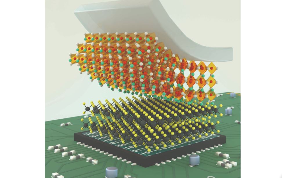
Researchers at Nanyang Technological University, Peking University, Tsinghua University, and the Beijing Academy of Quantum Information Sciences have recently demonstrated the successful integration of single-crystal strontium titrate, a high-κ perovskite oxide, with 2D semiconductors, using van der Waals forces. Their paper, published in Nature Electronics, could open new possibilities for the development of new types of transistors and electronic components.
“Our work was primarily inspired by a paper in Nature Materials published in 2016,” Wang Xiao Renshaw and Allen Jian Yang, two of the researchers who carried out the study, told TechXplore. “This paper introduced a smart approach to freestanding single-crystal perovskite films, which were typically viewed as fragile ceramics but have rich functionalities. This approach provides opportunities to transfer these materials on arbitrary substrates and integrates them with various materials.”
As one of the most promising perovskite oxides, SrTiO3 exhibits an extremely high dielectric constant. Integrating perovskite oxide with materials with different atomic structures, however, has been found to be almost impossible.
“Conventionally, the lattice mismatch between single-crystal perovskite oxides and 2D layered semiconductors hinders the epitaxial growth of high-quality oxide overlayers,” Renshaw and Yang explained. “Moreover, the conditions for the growth of single-crystal perovskite oxides, which involve high temperature and oxygen atmosphere, are detrimental to 2D layered semiconductors. However, in our van der Waals integration process, the perovskite oxides were grown on lattice-matched oxide substrates and then transferred onto 2D layered semiconductors at room temperature.”
Renshaw Wang, Yang and their colleagues had previously conducted several studies focusing on techniques to grow both oxides and 2D electronics. Building on the results they achieved in their previous works, they started trying to combine high-κ perovskite oxides and 2D layered semiconductors to create highly performing transistors.
To achieve this, the researchers grew the high-κ perovskite oxides on a water-dissolvable sacrificial layer. Subsequently, they lifted the perovskite oxides from this layer and transferred it onto two types of 2D semiconductors using elastomeric support (i.e., polydimethylsiloxane or PDMS). They specifically used molybdenum disulfide and tungsten diselenide, two different 2D semiconductors that allowed them to create n-type and p-type transistors, respectively.
Renshaw Wang and Yang evaluated the transistors they created in a series of tests and found that they attained remarkable results. Specifically, the molybdenum disulfide transistors exhibited an on/off current ratio of 108 at a supply voltage of 1 V and a minimum subthreshold swing of 66 mV dec-1.
“We successfully circumvented the limitations in the integration of high-κ perovskite oxide and 2D semiconductors and our approach could enable almost unlimited combinations of materials,” Renshaw Wang and Yang said. “In addition, we found the interface between transferred high-k perovskite oxides and MoS2 is of high quality, as it allowed us to fabricate field-effect transistors with abrupt subthreshold slopes.”
As part of their recent study, the researchers showed that the transistors they created could be used to fabricate high performing and low-power complementary metal-oxide-semiconductor CMOS inverter circuits. In the future, their devices could be manufactured on a large scale and used to develop logic circuits and microchips with lower power consumption.
“In our next studies, we will try to further improve the quality of the high-k perovskite oxide to decrease the supply voltage of the transistors and logic gates,” Renshaw and Yang added. “At the same time, we will monitor the gate leakage current and employ, if necessary, a buffer layer or double high-k oxides to block the gate leakage.” https://techxplore.com/news/2022-05-transistors-high-k-perovskite-oxides-2d.html


Recent Comments