One key objective of electronics engineering research is to develop computing devices that are both highly performing and energy-efficient, meaning that they can compute information quickly while consuming little power. One possible way to do this could be to combine units that perform logic operations and memory components into a single device.
So far, most computing devices have been made up of a processing unit and a physically separate memory component. The creation of a device that can efficiently perform both these functions, referred to as a logic-in-memory architecture, could help to significantly simplify devices and cut down their power consumption.
While a few of the logic-in-memory architectures proposed so far achieved promising results, most existing solutions come with practical limitations. For instance, some devices have been found to be unstable, unreliable or only applicable to specific use cases.
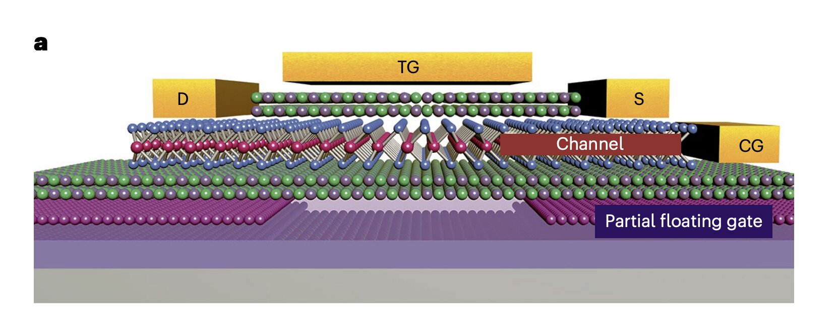
Researchers at Hunan University have recently developed a new reconfigurable logic-in-memory architecture based on a 2D van der Waals heterostructure, structures made up of isolated atomic layers bound together by the weak van der Waals interaction. Their device, introduced in a paper published in Nature Electronics, can work both as a reconfigurable transistor (i.e., device that can regulate, switch and amplify electrical signals) and as a reconfigurable memory component.
“We report a two-dimensional van der Waals heterostructure device that can function as both reconfigurable transistor and reconfigurable non-volatile memory, as well as provide reconfigurable logic-in-memory capabilities,” Xingxia Sun, Chenguang Zhu, Jiali Yi and their colleagues wrote in their paper. “The architecture of the device—termed a partial floating-gate field-effect transistor—offers both charge-trapping and field-regulating units.”
The logic-in-memory device created by Sun and her colleagues was termed a partial floating-gate field-effect transistor (PFGFET). It was fabricated using graphene (acting as the so-called floating gate), hexagonal boron nitride (hBN), and tungsten diselenide (WSe2).
Due to its unique design, the device can be easily reconfigured and switched to perform either memory or transistor functions. In initial tests, the researchers showed that it performs remarkably in both of these functions.
“When operating as a transistor, the device can be switched between the p- and n-type mode, and exhibits a subthreshold swing of 64 mV dec–1 and on/off current ratio approaching 108,” Sun, Zhu, Yi and their colleagues wrote in their paper. “When operating as a memory, the device can be switched between the p- and n-type memory and exhibits an erase/program ratio approaching 108.”
In the future, the new logic-in memory architecture proposed by this team of researchers could be used to create a variety of highly performing electronic devices, significantly lowering their power consumption. So far, Sun and her colleagues successfully used the PFGFETs they created to fabricate gates to perform both linear and nonlinear binary operations, but they could eventually be applied to a broader range of computations and operation patterns.
“We use the devices to fabricate complementary metal–oxide–semiconductor circuits, and linear and nonlinear logic gates with in situ storage, as well as device-efficient half-adder circuits,” the researchers explained in their paper. https://techxplore.com/news/2022-12-reconfigurable-device-based-2d-van.html


Recent Comments