


Two-dimensional (2D) semiconductor materials could enable the development of smaller yet highly performing electronic components, thus contributing to the advancement of a variety of devices. While significant strides have been made in the synthesis of 2D semiconductors with advanced electronic properties, their clean transfer onto substrates and reliable integration in real devices has so far proved challenging.
Researchers at Peking University, the Beijing Graphene Institute and other institutes in China have recently developed a new method to integrate 2D semiconductors with dielectric materials, which are insulating materials that help control the flow of electric charge in devices. Their approach, outlined in a paper published in Nature Electronics, entails the epitaxial growth of an ultra-thin dielectric film on a graphene-covered copper surface, which subsequently enables its transfer onto various substrates with minimal defects.
“The paper emerged from recognizing persistent challenges in integrating two-dimensional materials—such as graphene—into microelectronic devices,” Zhongfan Liu, Li Lin, and Yanfeng Zhang, corresponding authors of the paper, told Tech Xplore.
“Conventional transfer methods using polymer supports often introduce chemical contamination, mechanical stress, and interfacial defects, which compromise device performance. Our study was thus aimed at developing a comprehensive, wafer-scale process that overcomes these issues, by preserving graphene’s intrinsic properties and ensuring a clean, well-controlled interface during transfer and encapsulation.”
To demonstrate their newly proposed wafer-scale process, Lin and his colleagues first synthesized a single-crystal dielectric, namely antimony oxide (Sb2O3). They then deposited this dielectric on graphene that was grown on a Cu(111) substrate.
“Initially, Sb2O3 film is epitaxially grown on the graphene via a vacuum thermal evaporation process,” explained Lin. “The copper is then pre-treated with a water-ethanol mixture to form a thin oxide layer, reducing the adhesion between graphene and copper. The dielectric layer not only supports the transfer but also acts as the encapsulating layer, thereby protecting it from contamination and mechanical damage.”
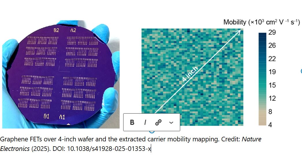
Notably, the researchers showed that the process enabled the reliable transfer of a 4-inch graphene wafer onto target substrates with minimal defects. In the future, this could open new possibilities for the development of new electronics that combine 2D semiconductors with dielectric materials.
“We realized the intact transfer of a 4‑inch graphene wafer with preserved intrinsic electrical properties (average carrier mobility of around 14,000 cm2 V-1 s-1) and integrated with single-crystal dielectric Sb2O3,” said Lin. “Remarkably, our method ensures excellent device uniformity and long-term stability, with minimal performance fluctuations observed even after prolonged air exposure.”
This recent work by Lin and his colleagues has notable practical implications, as the method they developed could soon enable the scalable fabrication of various highly performing and low-power microelectronics and optoelectronics based on 2D materials.
As part of their next studies, the researchers plan to build on their approach, while also trying to extend it to the 3D integration of 2D materials in real devices.
“We aim to develop advanced transfer techniques that facilitate the stacking and precise alignment of 2D materials to form multi-layer, three-dimensional integrated structures,” added Lin. “This research will focus on addressing challenges related to interlayer coupling, interface control, and patterning in 3D configurations, ultimately enabling the fabrication of high-performance, densely integrated electronic and optoelectronic devices.” https://techxplore.com/news/2025-04-approach-reliably-2d-semiconductors-dielectrics.html


Recent Comments