2D semiconductor tagged posts

Integrated Circuits based on a 2D Semiconductor Operating at GHz Frequencies

Integrated circuits based on a 2D semiconductor operating at GHz frequencies
High-performance MoS2 ring oscillator based on air-gap device structures. Credit: Fan et al

Transistors are crucial electronic components that regulate, amplify and control the flow of current inside most existing devices. In recent years, electronics engineers have been trying to identify materials and design strategies that could help to further improve the performance of transistors, while also reducing their size.

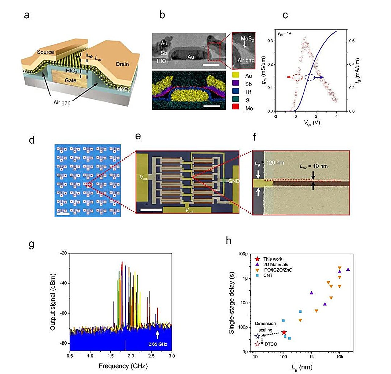
Two-dimensional (2D) transition metal dichalcogenides have some advantageous properties that could help to enhance the capabilities of transistors. While past studies have demonstrated the potential of these materials in individual transistors, their use for developing entire integrated circuits (ICs) that operate at high frequencies has proved challenging.

Researc...

Read More

Electronic Bridge allows Rapid Energy Sharing between Semiconductors

Artistic depiction of electron transfer driven by an ultrashort laser pulse, across an interface between two atomically-thin materials.
Artistic depiction of electron transfer driven by an ultrashort laser pulse, across an interface between two atomically-thin materials. This transfer is facilitated by an interlayer ‘bridge’ state that electrons are able to access due to lattice vibrations in both materials. (Credit: Gregory M. Stewart/SLAC)

As semiconductor devices become ever smaller, researchers are exploring two-dimensional (2D) materials for potential applications in transistors and optoelectronics. Controlling the flow of electricity and heat through these materials is key to their functionality, but first we need to understand the details of those behaviors at atomic scales.

Now, researchers have discovered that electrons play a surprising role in how energy is transferred between layers of 2D semiconductor m...

Read More

Single Photon Switch Advance

The ability to turn on and off a physical process with just one photon is a fundamental building block for quantum photonic technologies. Realizing this in a chip-scale architecture is important for scalability, which amplifies a breakthrough by City College of New York researchers led by physicist Vinod Menon. They’ve demonstrated for the first time the use of “Rydberg states” in solid state materials (previously shown in cold atom gases) to enhance nonlinear optical interactions to unprecedented levels in solid state systems. This feat is a first step towards realizing chip-scale scalable single photon switches.

In solid state systems, exciton-polaritons, half-light half-matter quasiparticles, which result from the hybridization of electronic excitations (excitons) and photons, a...

Read More

Graphene key to growing 2D Semiconductor with extraordinary properties

Graphene key to growing 2-dimensional semiconductor with extraordinary properties

An illustration of the Migration Enhance Encapsulated Growth (MEEG) process to stabilize novel wide-bandgap two-dimensional nitride semiconductors that are not naturally occurring. MEEG is facilitated by defects in the graphene lattice that act as pathways for intercalation. When the gallium and nitrogen adatoms meet at the graphene/SiC interface, they chemically react to form two-dimensional gallium nitride. Credit: Z. Al Balushi and Stephen Weitzner, Penn State MatSE

A newly discovered method for making two-dimensional materials could lead to new and extraordinary properties, particularly in nitrides, say the Penn State materials scientists who discovered the process...

Read More