2D semiconductors tagged posts

Next-Generation Sustainable Electronics are Doped with Air

Sheet of glass with light underneath.
Next-generation sustainable electronics are doped with air.Thor Balkhed

Semiconductors are the foundation of all modern electronics. Now, researchers at Linköping University, Sweden, have developed a new method where organic semiconductors can become more conductive with the help of air as a dopant. The study, published in the journal Nature, is a significant step towards future cheap and sustainable organic semiconductors.

“We believe this method could significantly influence the way we dope organic semiconductors. All components are affordable, easily accessible, and potentially environmentally friendly, which is a prerequisite for future sustainable electronics,” says Simone Fabiano, associate professor at Linköping University.

Semiconductors based on conductive plastics ins...

Read More

New Transistors integrating High-k Perovskite Oxides and 2D Semiconductors

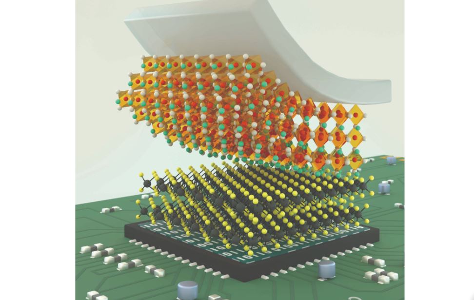
Over the past decades, electronics engineers and material scientists worldwide have been investigating the potential of various materials for fabricating transistors, devices that amplify or switch electrical signals in electronic devices. Two-dimensional (2D) semiconductors have been known to be particularly promising materials for fabricating the new electronic devices.

Despite their advantages, the use of these materials in electronics greatly depends on their integration with high-quality dielectrics, insulating materials or materials that are poor conductors of electrical current. These materials, however, can be difficult to deposit on 2D semiconductor substrates.

Researchers at Nanyang Technological University, Peking University, Tsinghua University, and the Beijing Acade...

Read More

Engineering 2D Semiconductors with Built-in Memory Functions

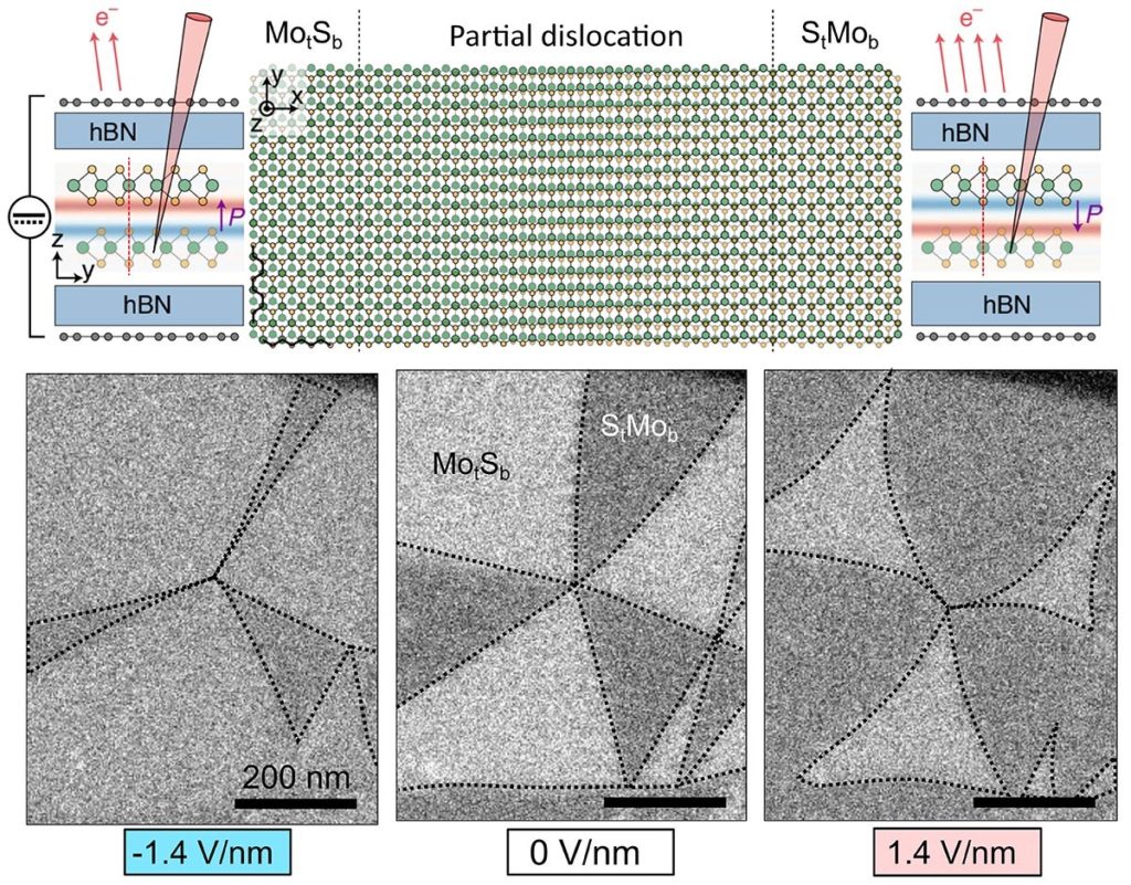
A team of researchers at The University of Manchester’s National Graphene Institute (NGI) and the National Physical Laboratory (NPL) has demonstrated that slightly twisted 2D transition metal dichalcogenides (TMDs) display room-temperature ferroelectricity.

This characteristic, combined with TMDs’ outstanding optical properties, can be used to build multi-functional optoelectronic devices such as transistors and LEDs with built-in memory functions on nanometre length scale.

Ferroelectrics are materials with two or more electrically polarisable states that can be reversibly switched with the application of an external electric field. This material property is ideal for applications such as non-volatile memory, microwave devices, sensors and transistors...

Read More

2D Semiconductors found to be close-to-ideal Fractional Quantum Hall Platform

Illustration of the monolayer WSe2 hosting "composite fermions"
A monolayer semiconductor is found to be a close-to-ideal platform for fractional quantum Hall state—a quantum liquid that emerges under large perpendicular magnetic fields. The image illustrates monolayer WSe2 hosting “composite fermions,” a quasi-particle that forms due to the strong interactions between electrons and is responsible for the sequence of fractional quantum Hall states.

Columbia University researchers report that they have observed a quantum fluid known as the fractional quantum Hall states (FQHS), one of the most delicate phases of matter, for the first time in a monolayer 2D semiconductor. Their findings demonstrate the excellent intrinsic quality of 2D semiconductors and establish them as a unique test platform for future applications in quantum computing...

Read More