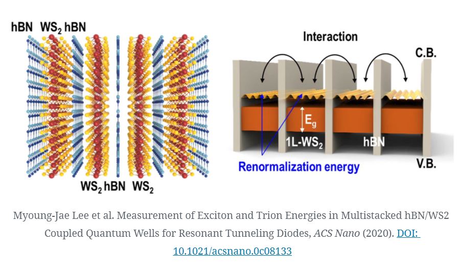
Scientists have designed a 2D material-based multi-stacked structure comprising tungsten disulfide (WS2) layer sandwiched between hexagonal boron nitride (hBN) layers that displays long-range interaction between successive WS2 layers with potential for reducing circuit design complexity and power consumption.
2D materials have been popular among materials scientists owing to their lucrative electronic properties, allowing their applications in photovoltaics, semiconductors, and water purification. In particular, the relative physical and chemical stability of 2D materials allow them to be “stacked” and “integrated” with each other...
Read More


Recent Comments