CMOS tagged posts

The Metalens meets the Stars – Large, All-glass Metalens Images Sun, Moon and Nebulae

image of the metalens and camera
This 10-centimeter-diameter glass metalens can image the sun, the moon and distant nebulae with high resolution. (Credit: Capasso Lab/Harvard SEAS)
 

Metalenses have been used to image microscopic features of tissue and resolve details smaller than a wavelength of light. Now they are going bigger.

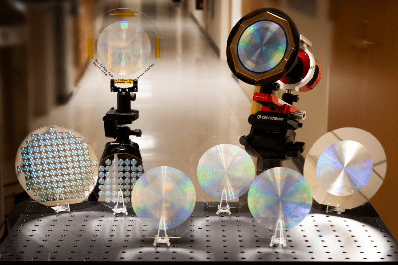
Researchers at the Harvard John A. Paulson School of Engineering and Applied Sciences (SEAS) have developed a 10-centimeter-diameter glass metalens that can image the sun, the moon and distant nebulae with high resolution.

It is the first all-glass, large-scale metalens in the visible wavelength that can be mass produced using conventional CMOS fabrication technology.

The research is published in ACS Nano.

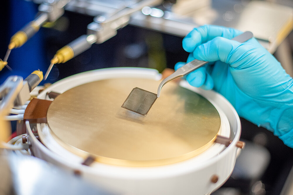
“The ability to accurately control the size of tens of billions of nanopill...

Read More

Conjoined ‘Racetracks’ make new Optical Device possible

Credit: Brian Long

Kerry Vahala and collaborators from UC Santa Barbara have found a unique solution to an optics problem. When we last checked in with Caltech’s Kerry Vahala three years ago, his lab had recently reported the development of a new optical device called a turnkey frequency microcomb that has applications in digital communications, precision time keeping, spectroscopy, and even astronomy.

This device, fabricated on a silicon wafer, takes input laser light of one frequency and converts it into an evenly spaced set of many distinct frequencies that form a train of pulses whose length can be as short as 100 femtoseconds (quadrillionths of a second). (The comb in the name comes from the frequencies being spaced like the teeth of a hair comb.)

Now Vahala (BS ’80, MS ’81,...

Read More

Scalable Method to Manufacture Thin Film Transistors achieves Ultraclean Interface

Scalable method to manufacture thin film transistors achieves ultra-clean interface for high performance, low-voltage device ope
Microchip containing thin film transistors having record sub-threshold slope, made using the in situ atomic layer deposition process. Credit: Silvia Cardarelli, Michigan ECE

Prof. Becky Peterson at the University of Michigan leads a team that has developed a scalable, manufacturable method for developing thin film transistors (TFTs) that operate at the lowest possible voltage. This is particularly important for TFT integration with today’s silicon complementary metal-oxide semiconductors (CMOS), which are used in the vast majority of integrated circuits.

“We’re essentially developing a less complicated device that operates at lower voltage,” said ECE Ph.D. student Tonglin (Tanya) Newsom, who is first author on the paper...

Read More

Building Energy-Efficient Computing Platforms

Building energy-efficient computing platforms
Images of the electronic platform used in the studies. Credit: CeNSE, IISc

The massive growth of data centers that consume enormous amounts of energy has contributed significantly to power shortages worldwide. With rising demand for faster and more intelligent computers and devices, there is a pressing need to develop alternatives to traditional electronic components that will make these devices more energy-efficient.

In two recent studies, researchers at the Centre for Nano Science and Engineering (CeNSE), IISc, report the development of a highly energy-efficient computing platform that offers promise in building next-generation electronic devices.

Instead of using complementary metal-oxide semiconductors (CMOS) which are the building blocks of most electronic circuits today, th...

Read More