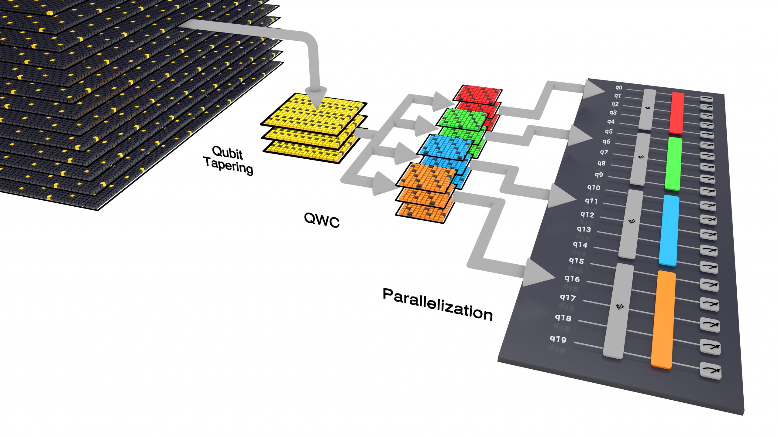
Using the full capabilities of the Quantinuum H1-1 quantum computer, resear...
Read More

July 31, 2023,
 Physics, Technology/Electronics
Using the full capabilities of the Quantinuum H1-1 quantum computer, resear...
Read More
May 7, 2017,
Chemistry/Nanotechnology, Physics, Technology/Electronics

A team of researchers, led by the University of Minnesota, have discovered a new nano-scale thin film material with the highest-ever conductivity in its class.
A new nano-scale thin film material with the highest-ever conductivity in its class has been found by a team of researchers, led by the University of Minnesota. The new material could lead to smaller, faster, and more powerful electronics, as well as more efficient solar cells. Besides high conductivity, it also has a wide bandgap, which means light can easily pass through the material making it optically transparent. In most cases, materials with wide bandgap, usually have either low conductivity or poor transparency.
“The high conductivity and wide bandgap make this an ideal material for making optically transparent conducting fil...
Read More
December 14, 2015,
Physics, Technology/Electronics

(Left) Silicon wires with match heads and (right) light absorption profile of a single match-head wire at 587 nm absorption. Credit: Image courtesy of the Center for Integrated Nanotechnologies
Crystal growth on a nano/microscale level produces “match-head”-like, 3D structures that enhance light absorption and photovoltaic efficiency. This is the first large structure grown on a nanowire tip and it creates a completely new architecture for harnessing energy. Match-head semiconductor nanowires focus incident light for greater overall efficiency. The match heads are naturally formed during the wire-growth process, which can be applied to various materials and structures for photonic and optoelectronic devices.
Enhanced light absorption and efficient, photogenerated carrier collection are...
Read More

Recent Comments