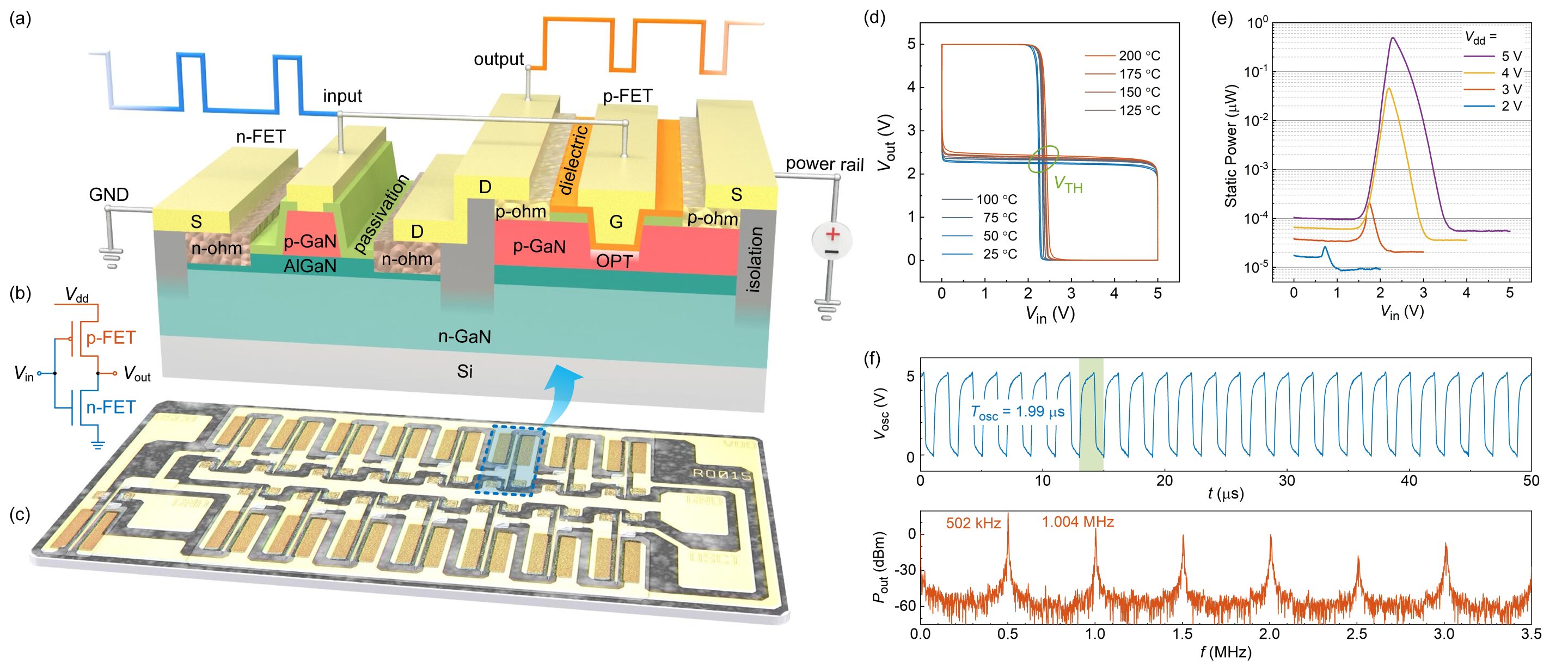
(a) Schematic view of the device structure of the GaN complementary logic inverter developed at HKUST; (b) corresponding circuit diagram; (c) perspective view of a true-color photo of the 15-stage GaN complementary ring oscillator fabricated in HKUST. (d) Cross-coupled plot of voltage transfer curves at different temperatures, and (e) static power dissipation with respect to different supply voltage and input voltage of the reported inverter. The inverter is very stable up to 200 °C with substantially large noise margins. (f) Oscillating waveform and the corresponding power spectrum of the reported ring oscillator. Credit: Zheng et al. (Springer Nature).
Most integrated circuits (ICs) and electronic components developed to date are based on silicon metal-oxide-semiconductor (CMOS) tec...


 Physics, Technology/Electronics

Recent Comments