


New research from the University of St Andrews paves the way for holographic technology, with the potential to transform smartdevices, communication, gaming and entertainment.
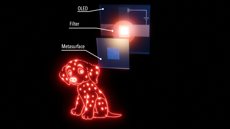
In a study published in Light: Science & Applications, researchers from the School of Physics and Astronomy created a new optoelectronic device from the combined use of holographic metasurfaces (HMs) and organic light-emitting diodes (OLEDs).
Until now, holograms have been created using lasers. However, researchers have found that using OLEDs and HMs gives a simpler and more compact approach that is potentially cheaper and easier to apply, overcoming the main barriers to hologram technology being used more widely.
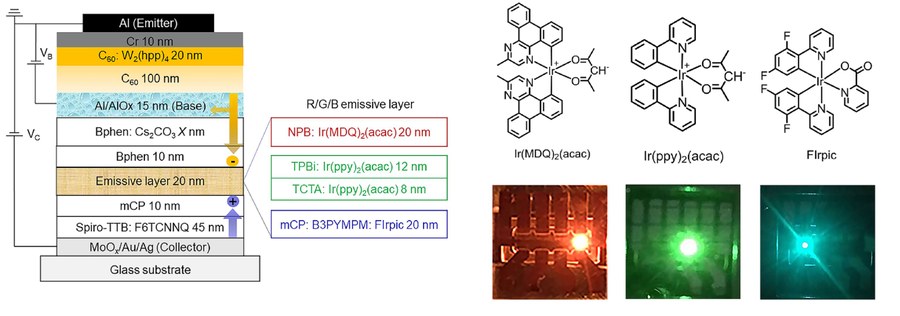
Organic light-emitting diodes are thin film devices widely used to make the colored pixels...
Read More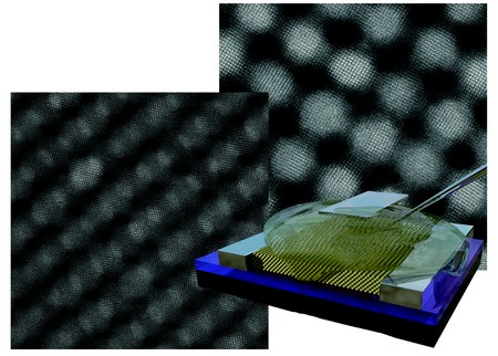


Recent Comments