

- A safer, more effective atrial fibrillation treatment method using magnetic gel may be on the way
- Self-repairing spacecraft could change future missions
- Injectable ‘satellite livers’ could offer an alternative to liver transplantation
- Next-generation memory material has the surprising property of shrinking when heated
plasmons tagged posts
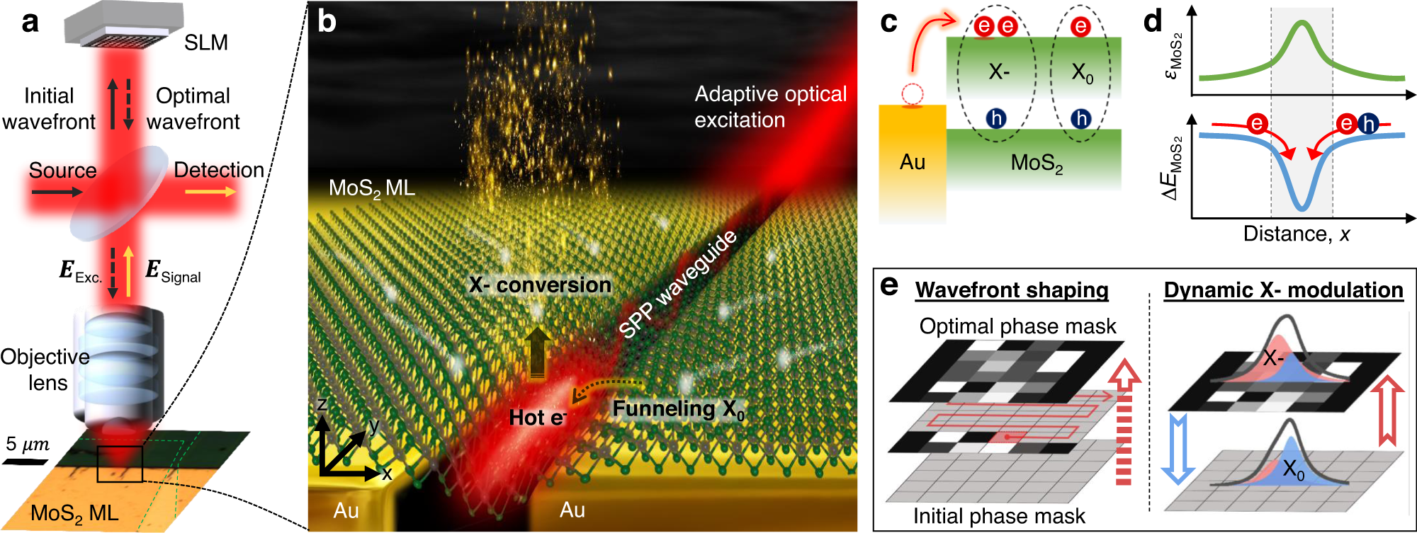
Team Manages to Dynamically Control Trions with a Waveguide
May 17, 2023,
 Physics, Technology/Electronics
Novel ‘Converter’ heralds breakthrough in Ultra-fast Data Processing at Nanoscale
October 21, 2017,
Physics, Technology/Electronics

A research team led by Associate Professor Christian Nijhuis from the Department of Chemistry at the NUS Faculty of Science (second from right) has recently invented a novel “converter” that can harness the speed and small size of plasmons for high frequency data processing and transmission in nanoelectronics.
Invention bagged 4 patents and could potentially make microprocessor chips work 1000X faster. Advancement in nanoelectronics has been fueled by the ever-increasing need to shrink the size of electronic devices in a bid to produce smaller, faster and smarter gadgets such as computers, memory storage devices, displays and medical diagnostic tools.
While most advanced electronic devices are powered by photonics – which involves the use of photons to transmit information – photonic e...
Read MoreQuantum Nanoscope: Seeing electrons surfing the waves of light on Graphene
June 9, 2017,
Physics, Technology/Electronics

Electrons and light are moving in concert along the graphene sheet.
Credit: ICFO/ F. Vialla
Researchers have studied how light can be used to “see” the quantum nature of an electronic material. They managed to do that by capturing light in a net of carbon atoms and slowing down light it down so that it moves almost as slow as the electrons in the graphene. Then something special happens: electrons and light start to move in concert, unveiling their quantum nature at such large scale that it could observed with a special type of microscope.
The experiments were performed with ultra-high quality graphene...
Read MoreLighting the Way to Miniature devices
September 14, 2016,
Physics, Technology/Electronics

A schematic (left) and photograph (right) of a photonic dew point temperature sensor developed by Ji Fang Tao and co-workers, which works by detecting changes in the refraction of light as water molecules condense onto the device. (left) © 2015 IEEE. Reprinted, with permission, from Ref 1. (right) © 2016 A*STAR Institute of Microelectronics
Electromagnetic waves created on a layer of organic molecules could provide the perfect on-chip light source for future quantum communication systems...
Read More

Recent Comments