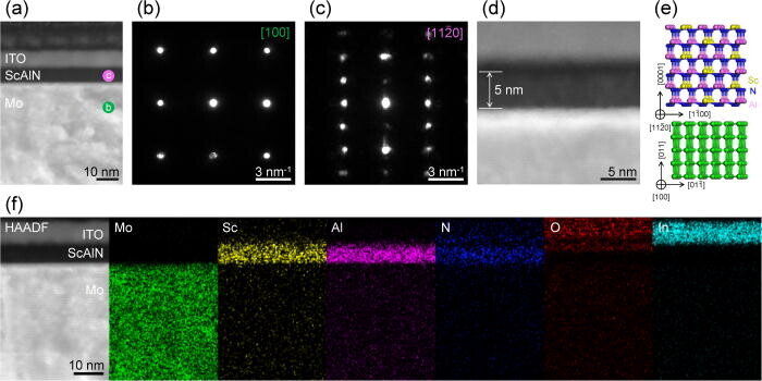
a) Cross-sectional HAADF-STEM image of the 5 nm thick ScAlN grown on Mo template. (b) and (c) Nano-beam electron diffraction patterns captured from the Mo (b) and ScAlN (c) regions labeled in (a). (d) Magnified HAADF-STEM image showing the thickness of the ScAlN layer. (e) Schematic of the epitaxial relationship between wz-ScAlN and bcc-Mo. (f) EDS element maps for the ITO/ScAlN/Mo capacitor. Credit: Applied Physics Letters (2023). DOI: 10.1063/5.0136265
Ferroelectric semiconductors are contenders for bridging mainstream computing with next generation architectures, and now a team at the University of Michigan has made them just five nanometers thick—a span of just 50 or so atoms.
This paves the way for integrating ferroelectric technologies with conventional components used in ...


Recent Comments