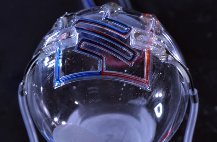
sensors tagged posts

New study reveals a Graphene Sheet behaves ‘Like a mirror’ for water molecules

An image showing graphene water molecules on both sides of graphene. Because graphene is a conductor of electricity, water molecules on both sides of the graphene attract each other by the same charges. (Courtesy image)

A recently published study led by Virginia Commonwealth University researchers sheds new light on how water interacts with the nanomaterial graphene, a single, thin layer of carbon atoms arranged in a hexagonal honeycomb lattice.

The researchers’ findings could hold implications for a variety of applications, including sensors, fuel cell membranes, water filtration, and graphene-based electrode materials in high-performance supercapacitors.

The study, “Solvent–Solvent Correlations across Graphene: The Effect of Image Charges,” was published in the American Chemica...

Read More

Twisting 2D materials uncovers their superpowers

three different interlayer twist angles and their subsequent crystalline symmetry
The twist angle between the layers governs the crystal symmetry and can lead to a variety of interesting physical behaviours, such as unconventional superconductivity, tunnelling conductance, nonlinear optics and structural super-lubricity.

Researchers can now grow twistronic material at sizes large enough to be useful. While an exciting potential area of nanotechnology, twistronics until now has mostly been explored on samples smaller than human hairs. Now researchers can produce samples on the centimetre scale.

2D materials, which consist of a single layer of atoms, have attracted a lot of attention since the isolation of graphene in 2004...

Read More

How do you Power Billions of Sensors? By Converting Waste Heat into Electricity

This image shows the external appearance of the developed compact, ultra-lightweight flexible thermoelectric conversion device. Credit: Osaka University

Interconnected healthcare and many other future applications will require internet connectivity between billions of sensors. The devices that will enable these applications must be small, flexible, reliable, and environmentally sustainable. Researchers must develop new tools beyond batteries to power these devices, because continually replacing batteries is difficult and expensive.

In a study published in Advanced Materials Technologies, researchers from Osaka University have revealed how the thermoelectric effect, or converting temperature differences into electricity, can be optimally used to power small, flexible devices...

Read More

Method Detects Defects in 2D Materials for future Electronics, Sensors

A yellow laser beam shines on a chip and reveals a grain boundary defect
A laser beam (yellow) reflects off a 2D material (orange) highlighting a grain boundary defect in the atomic lattice.
 IMAGE: MRI/PENN STATE

To further shrink electronic devices and to lower energy consumption, the semiconductor industry is interested in using 2D materials, but manufacturers need a quick and accurate method for detecting defects in these materials to determine if the material is suitable for device manufacture. Now a team of researchers has developed a technique to quickly and sensitively characterize defects in 2D materials.

Two-dimensional materials are atomically thin, the most well-known being graphene, a single-atom-thick layer of carbon atoms.

“People have struggled to make these 2D materials without defects,” said Mauricio Terrones, Verne M...

Read More