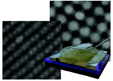
Electron microscope images showing two of the ordered structures formed in the experiments. Atoms inside the quantum dots are resolved by the microscope and it can be seen that they are aligned throughout adjacent dots. A model of the device used for the measurement of the electronic properties is shown in the bottom right. The superlattice lies between two electrodes while an ionic gel on top (gate electrode) is used to accumulate carriers in the active material. | Illustration Jacopo Pinna
Finding paves the way for new generation of opto-electronic applications. Quantum dots are clusters of some 1,000 atoms which act as one large ‘super-atom’. It is possible to accurately design the electronic properties of these dots just by changing their size...


Recent Comments