

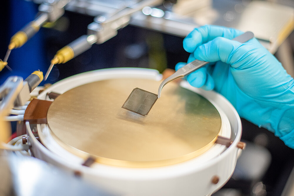
Prof. Becky Peterson at the University of Michigan leads a team that has developed a scalable, manufacturable method for developing thin film transistors (TFTs) that operate at the lowest possible voltage. This is particularly important for TFT integration with today’s silicon complementary metal-oxide semiconductors (CMOS), which are used in the vast majority of integrated circuits.
“We’re essentially developing a less complicated device that operates at lower voltage,” said ECE Ph.D. student Tonglin (Tanya) Newsom, who is first author on the paper...
Read More
Recent Comments