


Things do not always go as one wants in reality. This is especially true in the world of light. However, a research team at POSTECH has successfully controlled “trions,” a breakthrough toward developing what could ultimately be revolutionary optical communication technology.
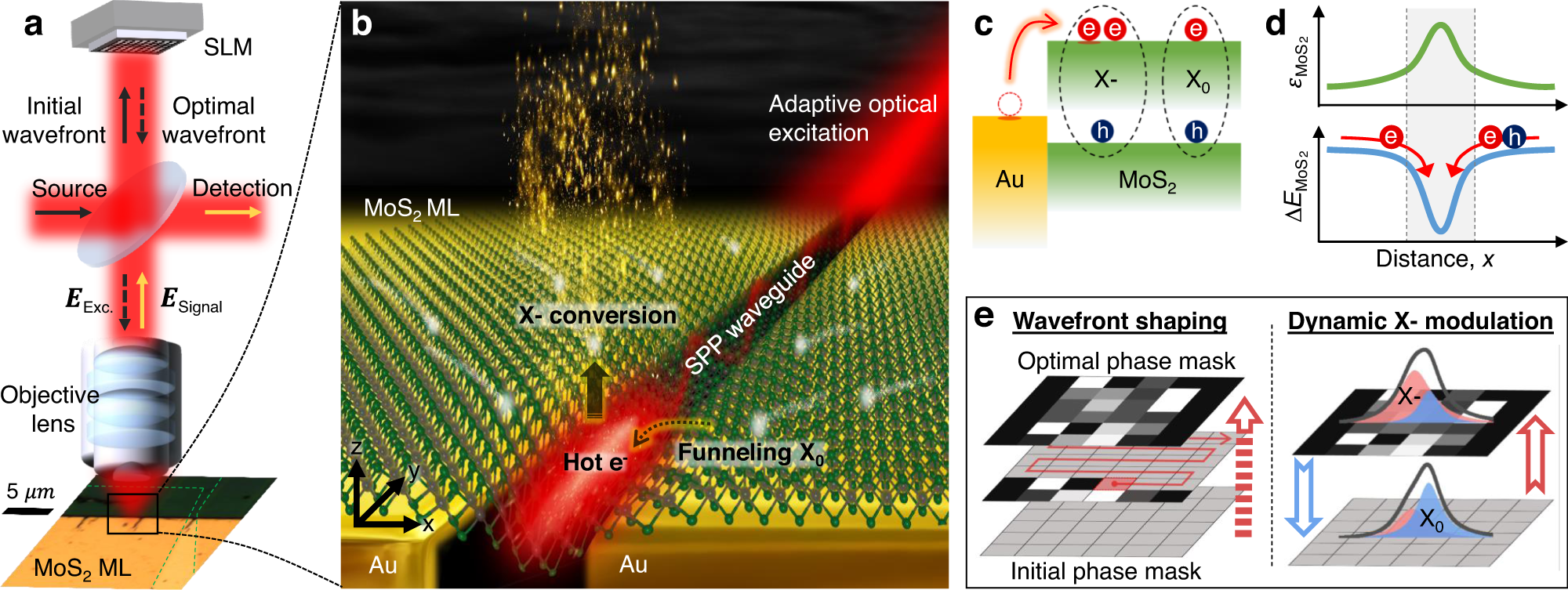
The team of researchers led by Professor Kyoung-Duck Park and Ph.D. candidate Hyeongwoo Lee in the Department of Physics at POSTECH has succeeded in producing high purity trions by using a nanoscale plasmonic waveguide and controlling the location at which the particles were created.
Excitons are formed when light is focused on semiconductor material. The exciton, a binding of an electron and a hole, is electrically neutral. Addition of one more electron to an exciton makes a trion. Even though both particles are used to make next-generation optical communications devices and solar cells, trions afford more advantages over excitons. They are better for practical device applications as they are controllable with an electric field and have a weaker binding energy.
The team used a “nanoscale plasmonic waveguide” with gap width of about 200 nm to create trions. The waveguide helps change light into “plasmons,” a phenomenon of collective electron oscillations. It also strongly confines plasmons in a space that is smaller than the wavelength of light to transport them to the desired location.
When a two-dimensional semiconductor material is transferred onto the waveguide, the material is stretched up along the groove on the waveguide. Focusing light onto the 2D material will form excitons in the semiconductor, and they flow to the center of the waveguide just like water poured through a funnel. The high energy of plasmons helps transport the electrons in the metal part of the waveguide toward the semiconductor. The transported electrons then move toward the center of the waveguide to bond with excitons, ultimately creating trions.
The team also successfully controlled the location where trions are created by spatially controlling plasmons with the combination of adaptive optics and nano optics. With this technology, the researchers were able to produce both plasmons and trions at the desired location on the plasmonic waveguide.
This research is significant in that “light” was employed instead of “electricity”. The passage that light moves along helped find a solution to development of optical devices. It is also meaningful that the research brought together different disciplines: “excitonics” that studies particles such as excitons and “plasmonics” that explores plasmons. When facing our limits, we tend to find a solution within our field. However, the team thought outside the box to find a solution based on convergence of different disciplines.
The research findings are expected to greatly contribute to efficient control of trion-based optical devices and development of highly-efficient devices for optically converting energy. Hyeongwoo Lee, the first author of the paper, said, “I think the research defined a new physical concept that can create and control trions in nanoscale spaces. Based on the research outcome, I am sketching out research on a wide area information and communication technology with semiconductor particles.”
The plasmonic waveguide was fabricated by a team led by Hyuck Choo, executive vice president of Samsung Electronics; the pre-analysis of the samples was conducted by a team led by Professor Hong Seok Lee and Professor Sangmin An of Jeonbuk National University; the materials used in the experiment were prepared by a team led by Professor Ki Kang Kim of Sungkyunkwan University; and measurements were conducted together with Yeonjeong Koo, Huitae Joo, and Mingu Kang of the Department of Physics at POSTECH.
The research is published in the journal Nature Communications.
https://www.nature.com/articles/s41467-023-37481-1


Recent Comments