Quantum entanglement refers to a phenomenon in quantum mechanics in which two or more particles become linked such that the state of each particle cannot be described independently of the others, even when they are separated by a large distance. The principle, referred to by Albert Einstein as “spooky action at a distance,” is now utilized in quantum networks to transfer information. The building blocks of these networks—quantum nodes—can generate and measure quantum states.
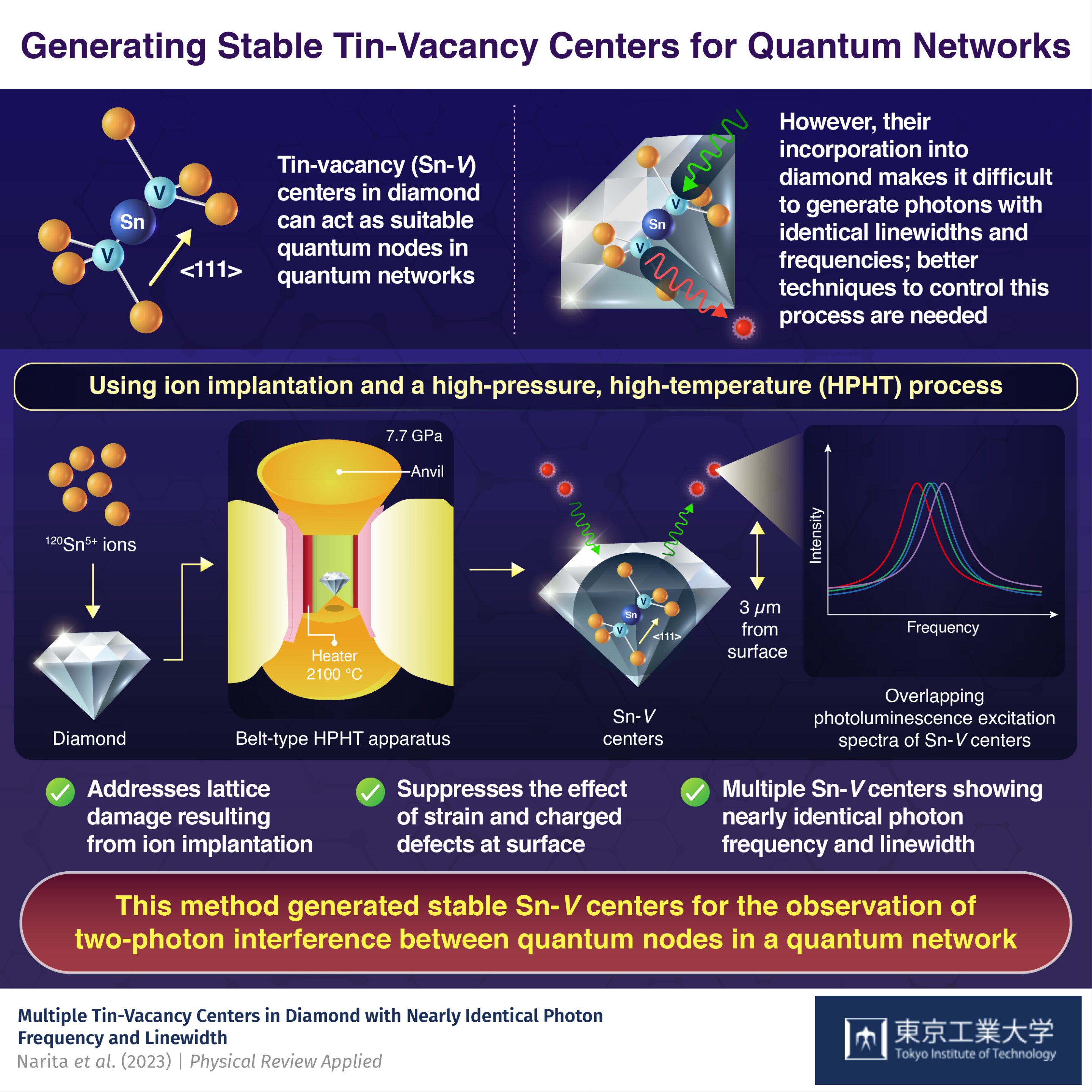
Among the candidates that can function as quantum nodes, the Sn-V center in diamond (a defect where a tin (Sn) atom replaces a carbon atom, resulting in an interstitial Sn atom between two carbon vacancies) has been shown to have suitable properties for quantum network applications.
The Sn-V center is expected to exhibit a long spin coherence time in the millisecond range at Kelvin temperatures, allowing it to maintain its quantum state for a relatively long period of time. However, these centers have yet to produce photons with similar characteristics, which is a necessary criterion for creating remote entangled quantum states between quantum network nodes.
Now in a study published in Physical Review Applied, researchers led by Associate Professor Takayuki Iwasaki from Tokyo Institute of Technology (Tokyo Tech), Japan, have observed Sn-V centers with identical photon frequency and linewidth, marking a new phase in the use of these centers as quantum nodes.
“Control of the linewidth and wavelength is challenging in solid-state materials. This is especially true for Sn-V centers—which are composed of heavy atoms—because their incorporation in diamond causes more defects and higher strain around emitters,” says Dr. Iwasaki.
The researchers used a combination of ion implantation, and high-pressure-high-temperature (HPHT) annealing to form Sn-V centers in diamond. Ion implantation was used to implant Sn ions into diamond substrates.
These samples were then exposed to high temperatures of 2100 °C and high pressures of 7.7 GPa in a belt-type apparatus. With this two-step process, the researchers eliminated the effects of surface defects and strain on the optical properties of the Sn-V centers and addressed issues with defects normally faced when generating the Sn-V centers.
“The high-temperature treatment efficiently addressed the lattice damage. Consequently, the strain around the emitters was largely suppressed. Moreover, the Sn-V centers were formed at a depth of approximately 3 micrometers from the surface of the samples. This suppressed the effect of strain and charged defects at the surface, potentially shifting the energy level of the emitters,” says Dr. Iwasaki.
On subsequently scanning the different areas of the sample with a narrow linewidth tunable laser and analyzing the emitted light, the team observed multiple Sn-V centers with nearly identical photon frequencies and linewidths, marking the successful formation of stable Sn-V centers which were suitable for use as quantum nodes.
Dr. Iwasaki is optimistic about the future implications of their work. “The formation of high-quality Sn-V centers directly leads to the observation of two-photon interference between distant emitters and the future establishment of Sn-V centers in diamond as a quantum-light matter interface,” he says. https://phys.org/news/2023-02-breakthrough-tin-vacancy-centers-quantum-network.html


Recent Comments