
Category Chemistry/Nanotechnology

Wonder Material? Novel Nanotube structure Strengthens Thin Films for Flexible Electronics

Scanning Electron Microscope Images of architectured carbon nanotube (CNT) textile made at Illinois. Colored schematic shows the architecture of self-weaved CNTs, and the inset shows a high resolution SEM of the inter-diffusion of CNT among the different patches due to capillary splicing. Credit: University of Illinois

Scanning Electron Microscope Images of architectured carbon nanotube (CNT) textile made at Illinois. Colored schematic shows the architecture of self-weaved CNTs, and the inset shows a high resolution SEM of the inter-diffusion of CNT among the different patches due to capillary splicing. Credit: University of Illinois

Reflecting the structure of composites found in nature and the ancient world, researchers at the University of Illinois at Urbana-Champaign have synthesized thin carbon nanotube (CNT) textiles that exhibit both high electrical conductivity and a level of toughness that is about 50X higher than copper films, currently used in electronics...

Read More
Scientific advance for Cool Clothing: Temperature-wise, that is

Stanford University cool material

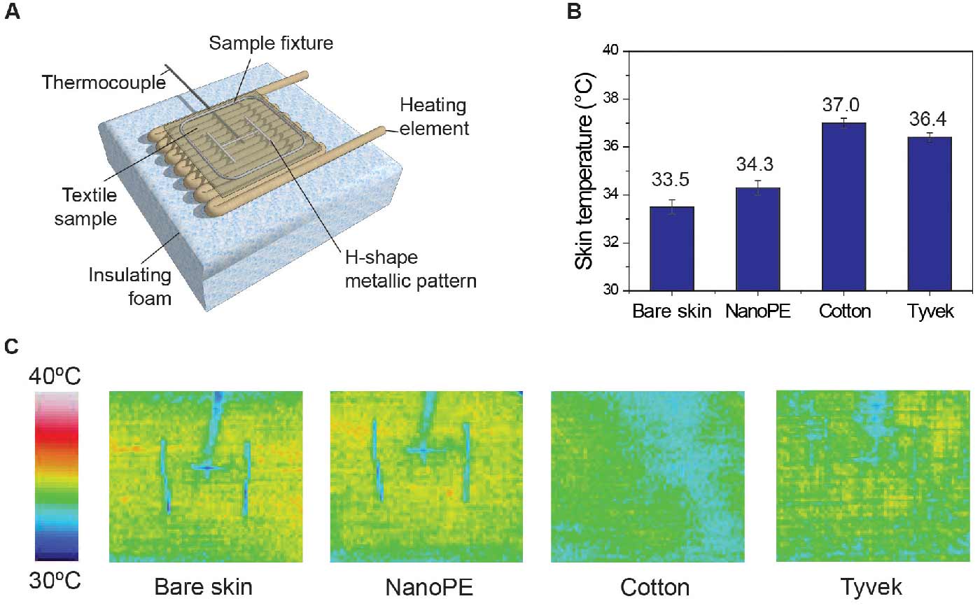
Thermal measurement of nanopolyethylene (nanoPE) and various textile samples. (A) experimental setup of textile thermal measurement. The heating element that generates constant heating power is used to simulate human skin, and the “skin temperature” is measured with the thermocouple. Lower skin temperature means a better cooling effect. (B) Thermal measurement of bare skin, nanoPE, cotton, and Tyvek. NanoPE has a much better cooling effect than that of cotton and Tyvek because of its infrared (IR)-transparency. (C) Thermal imaging of bare skin and the three samples. Only nanoPE can reveal the H-shape metallic pattern because of its IR-transparency. Photo by Stanford University.

Stanford University researchers, with the aid of the Comet supercomputer at the San Diego Supercomputer at UCSD, ...

Read More

Graphene ‘Copy Machine’ may produce Cheap Semiconductor Wafers

(Left to right): Postdoc Kyusang Lee, Professor Jeehwan Kim (sitting), and graduate students Samuel Cruz and Yunjo Kim. Credit: Jose-Luis Olivares/MIT

(Left to right): Postdoc Kyusang Lee, Professor Jeehwan Kim (sitting), and graduate students Samuel Cruz and Yunjo Kim. Credit: Jose-Luis Olivares/MIT

A new technique may vastly reduce the overall cost of wafer technology and enable devices made from more exotic, higher-performing semiconductor materials than conventional silicon. The new method uses graphene as a sort of ‘copy machine’ to transfer intricate crystalline patterns from an underlying semiconductor wafer to a top layer of identical material. In 2016, annual global semiconductor sales reached their highest-ever point, at $339 billion worldwide. In that same year, the semiconductor industry spent about $7...

Read More

Degradable Electronic Components created from Corn Starch

Degradable Poly(lactic acid)/Metal–Organic Framework Nanocomposites Exhibiting Good Mechanical, Flame Retardant, and Dielectric Properties for the Fabrication of Disposable Electronics

Degradable Poly(lactic acid)/Metal–Organic Framework Nanocomposites Exhibiting Good Mechanical, Flame Retardant, and Dielectric Properties for the Fabrication of Disposable Electronics

As consumers upgrade their gadgets at an increasing pace, the amount of electronic waste we generate continues to mount. To help combat this environmental problem, researchers have modified a degradable bioplastic derived from corn starch or other natural sources for use in more eco-friendly electronic components. They report their development in ACS’ journal Industrial & Engineering Chemistry Research.

In 2014, consumers around the world discarded about 42 million metric tons of e-waste, according to a report by the United Nations University...

Read More