The illustration shows the cross-section of a thermal bimorph mirror and its constituents. Controlling the temperature of the mirror changes the curvature of the reflected wavefront. Overlaid on the cross-section is the simulated radial stress, showing a concentration of stress at the boundary of the two layers, where the adhesive holds the structure together. Credit: Huy Tuong Cao, University of Adelaide
Improved deformable mirrors could help scientists detect new sources of gravitational waves from deep in space. Researchers have developed a new type of deformable mirror that could increase the sensitivity of ground-based gravitational wave detectors such as the Advanced Laser Interferometer Gravitational-Wave Observatory (LIGO)...
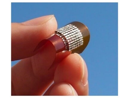
This image shows the external appearance of the developed compact, ultra-lightweight flexible thermoelectric conversion device. Credit: Osaka University
Interconnected healthcare and many other future applications will require internet connectivity between billions of sensors. The devices that will enable these applications must be small, flexible, reliable, and environmentally sustainable. Researchers must develop new tools beyond batteries to power these devices, because continually replacing batteries is difficult and expensive.
In a study published in Advanced Materials Technologies, researchers from Osaka University have revealed how the thermoelectric effect, or converting temperature differences into electricity, can be optimally used to power small, flexible devices...
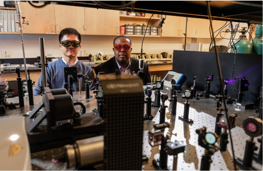
Researchers Cheng Zhe and Samuel Graham shown with an optical test setup for studying gallium nitride devices cooled by placement on a diamond substrate. (Credit: Rob Felt, Georgia Tech)
A room-temperature bonding technique for integrating wide bandgap materials such as gallium nitride (GaN) with thermally-conducting materials such as diamond could boost the cooling effect on GaN devices and facilitate better performance through higher power levels, longer device lifetime, improved reliability and reduced manufacturing costs. The technique could have applications for wireless transmitters, radars, satellite equipment and other high-power and high-frequency electronic devices.
The technique, called surface-activated bonding, uses an ion source in a high vacuum environment to first ...
New chip-based devices contain all the optical components necessary for quantum key distribution. The cost-effective platform is designed to facilitate citywide networks. Credit: Henry Semenenko, University of Bristol
Researchers have demonstrated new chip-based devices that contain all the optical components necessary for quantum key distribution while increasing real-world security. The fast and cost-effective platform is poised to facilitate implementation of extremely secure data communication that can be used to protect everything from emails to online banking information.
Advances in computing technology will soon leave today’s methods for encrypting online data vulnerable to eavesdropping...






Recent Comments