

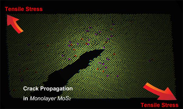
Schematic representation of the crack propagation in 2D MoS2 at the atomic level. Dislocations shown with red and purple dots are visible at the crack tip zone. Internal tensile stresses are represented by red arrows.
Cracks sank the ‘unsinkable’ Titanic; decrease the performance of touchscreens and erode teeth. We are familiar with cracks in 3D objects, but how do thin 2D materials crack? 2D materials, like molybdenum disulfide (MoS2), have emerged as an important asset for future electronic and photoelectric devices. However, the mechanical properties of 2D materials are expected to differ greatly from 3D materials...
Read More


Recent Comments