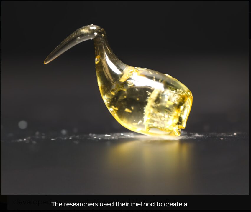
A focus-stacked macro photograph of a fabricated gallium phosphide photonic chip featuring multiple spiral waveguides and other test structures. The chip width is just 0.55 cm across. Due to the high Kerr nonlinearity of gallium phosphide, its high refractive index, and its negligible two-photon absorption, extremely efficient optical parametric amplification and frequency conversion over S, C, and L optical communication bands are achieved using this chip. Credit: Nikolai Kuznetsov (EPFL).
Modern communication networks rely on optical signals to transfer vast amounts of data. But just like a weak radio signal, these optical signals need to be amplified to travel long distances without losing information.
The most common amplifiers, erbium-doped fiber amplifiers (EDFAs), have served...
A simple, energy-efficient 3D-printing process takes its cues from trees to manufacture polymers quickly and inexpensively. Charging forward at top speed, a garden snail slimes up 1 millimeter of pavement per second. By this logic, Beckman Institute for Advanced Science and Technology researchers’ new 3D printing process speeds past existing methods — at a snail’s pace.
Researchers in Beckman’s Autonomous Materials Systems Group created “growth printing,” which mimics tree trunks’ outward expansion to print polymer parts quickly and efficiently without the molds and expensive equipment typically associated with 3D printing. Their work appears in the journal Advanced Materials.
“Humans are incredibly talented at making things...
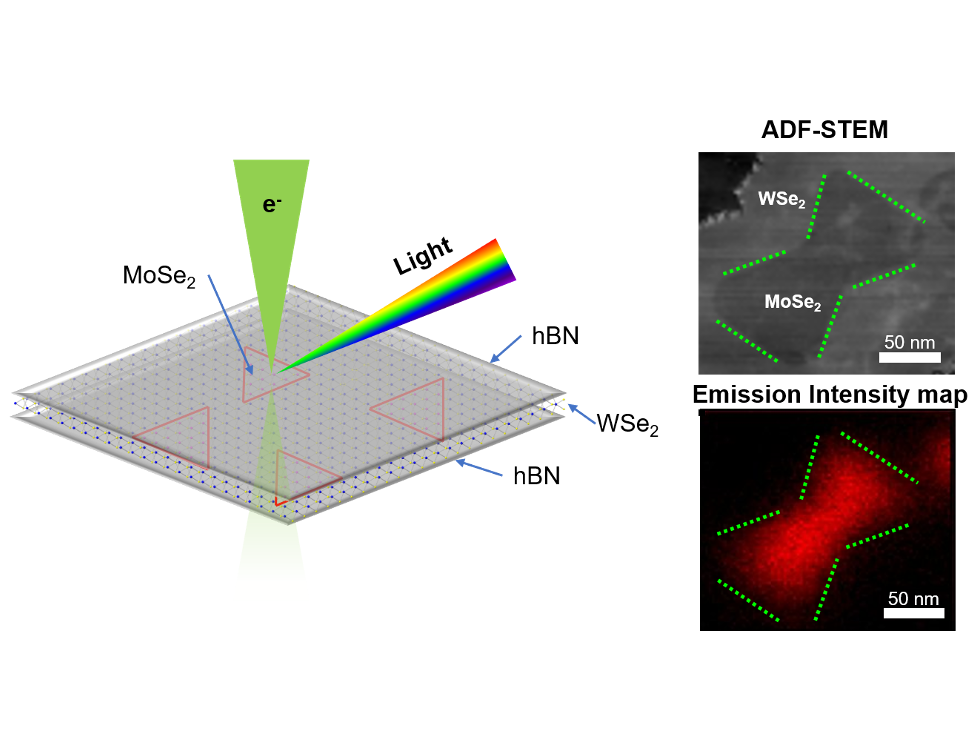
On the left is an illustration of the experimental setup from this study. Molybdenum diselenide nanodots, represented by red triangles, are embedded in tungsten diselenide and encapsulated by hexagonal boron nitride (hBN) on top and bottom. A focused electron beam, shown in green, in a scanning transmission electron microscope (STEM) is aimed at the structure. The emitted light is collected to generate an intensity map. On the upper right is adark-field STEM image of the molybdenum diselenide nanodot embedded inside tungsten diselenide. The contour of the nanodot is marked by dotted green lines. On the lower right is an artificially colored light emission intensity map of the same region, with the localized emission from the nanodot clearly visible. Credit: Provided by the researchers...Read More
Quantum tornado in momentum space: In the quantum material tantalum arsenide (TaAs), electrons form vortices in momentum space. Momentum space is a physics concept used to analyze how electrons behave in solids. A research team from the Cluster of Excellence ct.qmat at Würzburg and Dresden has now provided the first experimental evidence of these quantum tornadoes. (Image: think-design | Jochen Thamm)
A team of researchers from Würzburg has for the first time experimentally demonstrated a quantum tornado. Electrons form vortices in the momentum space of the quantum semi-metal tantalum arsenide.
Scientists have long known that electrons can form vortices in quantum materials...






Recent Comments