Category Technology/Electronics

New Antennas and Microchips help Electronics blur the line between Science and Sci-fi

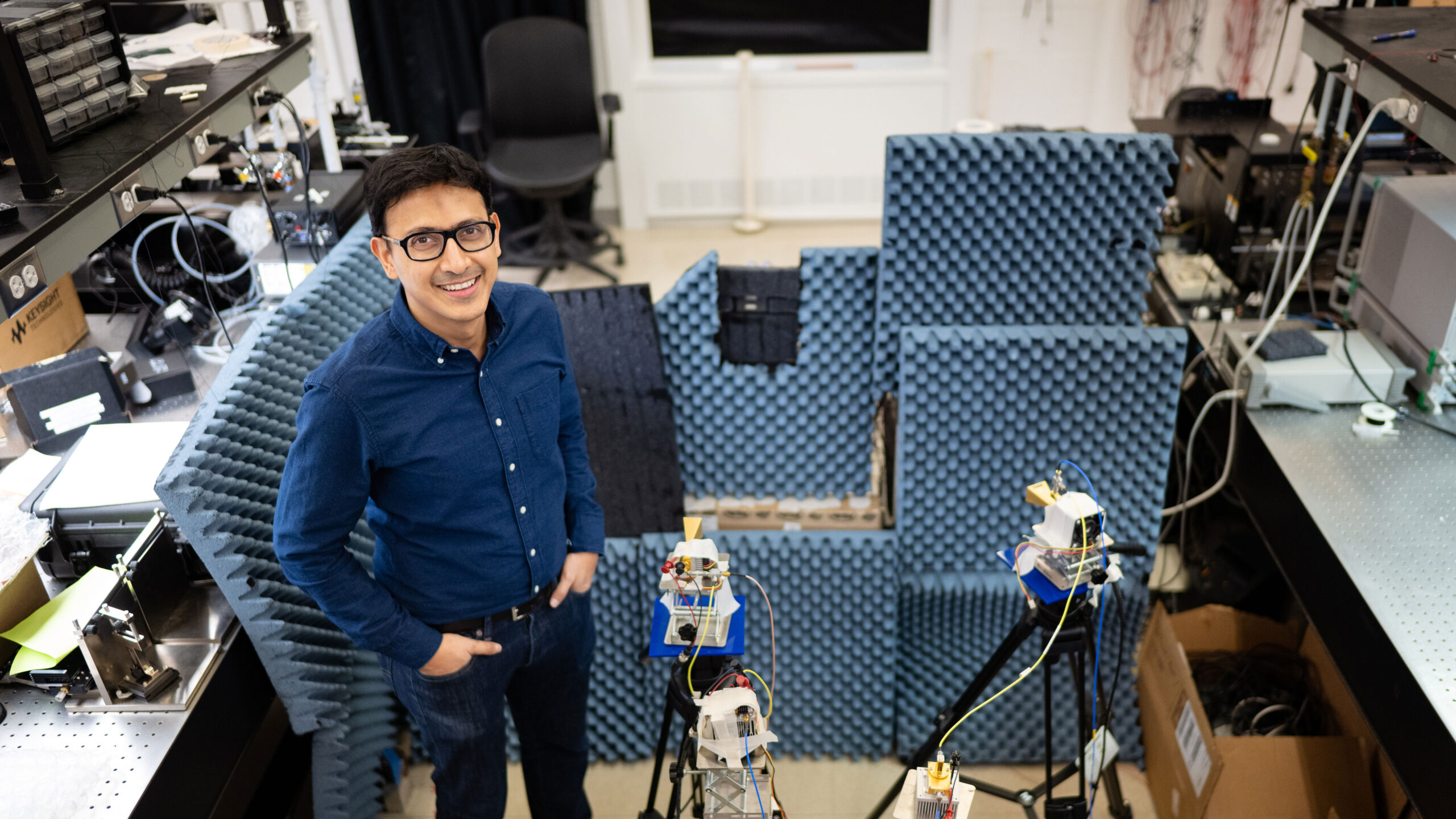
Kaushik Sengupta in his lab at Princeton
Researchers in Kaushik Sengupta’s lab work to expand the capabilities of modern electronics. Photos by Sameer A. Khan/Fotobuddy

Sophisticated antenna arrays paired with high-frequency wireless chips act like superpowers for modern electronics, boosting everything from sensing to security to data processing. In his lab at Princeton, Kaushik Sengupta is working to expand those powers even further.

In recent years, Sengupta’s lab has designed antenna arrays that help engineers make strides toward peering through matter, boosting communications in canyons of skyscrapers, putting a medical lab on a smart phone, and encrypting critical data with electromagnetic waves instead of software.

In a new article in Advanced Science, Sengupta’s research team presented a new type of antenna arra...

Read More
Approaching the Terahertz Regime

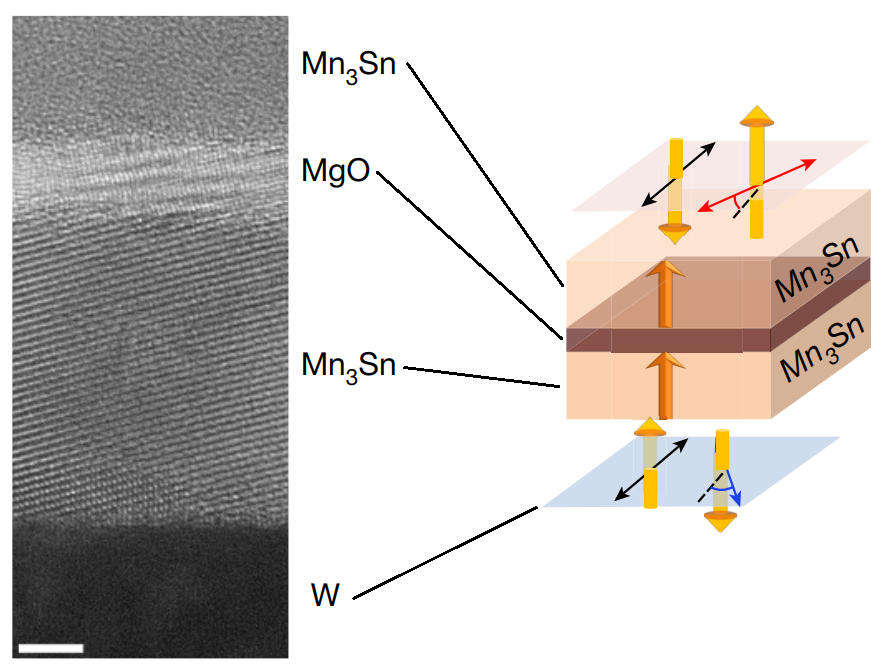
(Left) A chaotic greyscale rectangle. (Right) Isometric view of colored layers sandwiched together.
Antiferromagnetic tunneling junction. High-resolution transmission electron microscopy image of the antiferromagnetic junction showing layers of different materials (left). Diagram showing the materials’ magnetic properties (right). ©2023 Nakatsuji et al. CC-BY

Room temperature quantum magnets switch states trillions of times per second. A class of nonvolatile memory devices, called MRAM, based on quantum magnetic materials, can offer a thousandfold performance beyond current state-of-the-art memory devices. The materials known as antiferromagnets were previously demonstrated to store stable memory states, but were difficult to read from. This new study paves an efficient way for reading the memory states, with the potential to do so incredibly quickly too.

You can probably blink...

Read More

Engineers Grow ‘Perfect’ Atom-Thin Materials on Industrial Silicon Wafers

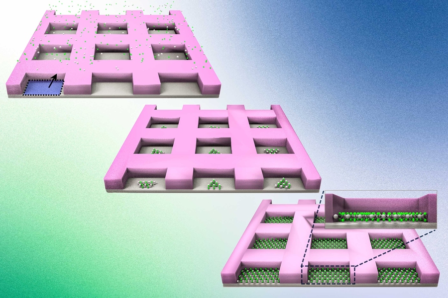
A pink wafer has square holes in a grid. The wafer is repeated 3 times. On top left, green and white atoms randomly float around the wafer. In the middle, the atoms line up inside the square holes in triangular formations. On the right, a closeup shows the perfectly lined-up rows of atoms.
Caption:By depositing atoms on a wafer coated in a “mask” (top left), MIT engineers can corral the atoms in the mask’s individual pockets (center middle), and encourage the atoms to grow into perfect, 2D, single-crystalline layers (bottom right).
Credits:Courtesy of the researchers. Edited by MIT News.

Their technique could allow chip manufacturers to produce next generation transistors based on materials other than silicon. Engineers fabricated 2D materials that could lead to next-generation transistors and electronic films.

True to Moore’s Law, the number of transistors on a microchip has doubled every year since the 1960s...

Read More

Scientists use Laser to Guide Lightning Bolt for First Time

Deflecting lightning with a laser lightning rod

Scientists said Monday they have used a laser beam to guide lightning for the first time, hoping the technique will help protect against deadly bolts—and one day maybe even trigger them.

Lightning strikes between 40-120 times a second worldwide, killing more than 4,000 people and causing billions of dollars worth of damage every year.

Yet the main protection against these bolts from above is still the humble lightning rod, which was first conceived by American polymath Benjamin Franklin in 1749.

A team of scientists from six research institutions have been working for years to use the same idea but replace the simple metal pole with a far more sophisticated and precise laser.

Now, in a study published in the journal Nature Photonics, they describe using a laser beam—shot...

Read More