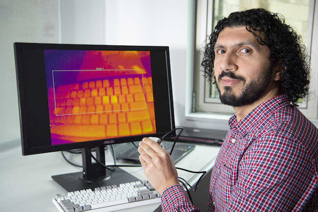
Category Technology/Electronics

The Laser Breakthrough that could make Tech even Faster

The laser breakthrough that could make tech even faster
The laser tool developed by the UQ team. Credit: Dr Martin Plöschner

Lasers have become a major part of our day-to-day lives. From phones and tablets to self-driving cars and data communication—even the information you’re reading right now is likely being delivered to you via lasers.

The technology’s applications are so broad even the researchers who deal with lasers daily are continuously amazed.

Among them is University of Queensland Research Fellow Dr. Martin Plöschner from the School of Information Technology and Electrical Engineering (ITEE).

“I’ve been working with lasers for the past 15 years and yet I’m often surprised to find them in the most unexpected places,” Dr. Plöschner said.

“In many of their applications, lasers operate in part of the spectrum which is...

Read More

Through the Quantum Looking Glass

Green laser light illuminates a metasurface that is a hundred times thinner than paper, that was fabricated at the Center for Integrated Nanotechnologies. CINT is jointly operated by Sandia and Los Alamos national laboratories for the Department of Energy Office of Science. (Photo by Craig Fritz) Click on the thumbnail for a high-resolution image.

A thin device triggers one of quantum mechanics’ strangest and most useful phenomena. An ultrathin invention could make future computing, sensing and encryption technologies remarkably smaller and more powerful by helping scientists control a strange but useful phenomenon of quantum mechanics, according to new research recently published in the journal Science.

Scientists at Sandia National Laboratories and the Max Planck Institute for the...

Read More

Unique Ferroelectric Microstructure revealed for first time

STEM image of polar nanoregions
An atomically resolved scanning transmission electron microscopy (STEM) image of the polar nanoregions (PNRs) embedded in the nonpolar matrix in the layered perovskite material (Ca, Sr)3Mn2O7. Bright contrast in the images can be directly interpreted as the atomic columns in the crystal. Aberration corrected STEM was employed to direct capture the arrangement of the atoms in the (a-type and b-type) polar nanoregions in the crystal and the displacement measurement at picometer precision were performed on the STEM images to extract the distortion in the structure. Credit: Alem Group/Jennifer M. McCann, MRI. All Rights Reserved.

A team of researchers have observed and reported for the first time the unique microstructure of a novel ferroelectric material, enabling the development of lead-...

Read More

Modified Microwave oven cooks up Next-gen Semiconductors

James Hwang
James Hwang, research professor in the Department of Materials Science and Engineering, right, at his modified microwave with Gianluca Fabi holding a semiconductor at left. Ryan Young/Cornell University

A household microwave oven modified by a Cornell engineering professor is helping to cook up the next generation of cellphones, computers and other electronics after the invention was shown to overcome a major challenge faced by the semiconductor industry.

The research is detailed in a paper published in Applied Physics Letters. The lead author is James Hwang, a research professor in the department of materials science and engineering.

As microchips continue to shrink, silicon must be doped, or mixed, with higher concentrations of phosphorus to produce the desired current...

Read More