
Category Technology/Electronics

An Organic Solar Cell with 25% Efficiency

The ‘best conversion performance in the world in a dark room’ is how the developers of a new organic PV device have described it. Such cells could be used as a wireless source of energy for IoT applications or in gadgets such as temperature-humidity and motion sensors.

Eight months ago, a state-funded French research institute and Japanese textiles company Toyobo announced they would join forces to develop superior organic solar cells for indoor applications. The partnership, the French organization said at the time, was aimed at developing thin, flexible solar cells which could function where conventional, inorganic solar cells could not.

The new energy technologies and nanomaterials (Liten) division of the French Alternative Energies and Atomic Energy Commission and To...

Read More
How do you Power Billions of Sensors? By Converting Waste Heat into Electricity

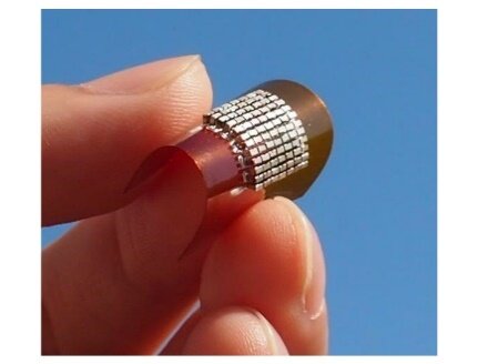
This image shows the external appearance of the developed compact, ultra-lightweight flexible thermoelectric conversion device. Credit: Osaka University

Interconnected healthcare and many other future applications will require internet connectivity between billions of sensors. The devices that will enable these applications must be small, flexible, reliable, and environmentally sustainable. Researchers must develop new tools beyond batteries to power these devices, because continually replacing batteries is difficult and expensive.

In a study published in Advanced Materials Technologies, researchers from Osaka University have revealed how the thermoelectric effect, or converting temperature differences into electricity, can be optimally used to power small, flexible devices...

Read More

Room-Temperature Bonded Interface improves Cooling of Gallium Nitride devices

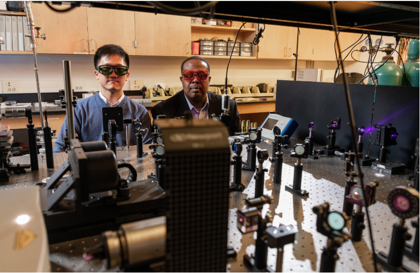
Researchers Cheng Zhe and Samuel Graham shown with an optical test setup for studying gallium nitride devices cooled by placement on a diamond substrate. (Credit: Rob Felt, Georgia Tech)

A room-temperature bonding technique for integrating wide bandgap materials such as gallium nitride (GaN) with thermally-conducting materials such as diamond could boost the cooling effect on GaN devices and facilitate better performance through higher power levels, longer device lifetime, improved reliability and reduced manufacturing costs. The technique could have applications for wireless transmitters, radars, satellite equipment and other high-power and high-frequency electronic devices.

The technique, called surface-activated bonding, uses an ion source in a high vacuum environment to first ...

Read More

Chip-based Devices Improve Practicality of Quantum-Secured Communication

New chip-based devices contain all the optical components necessary for quantum key distribution. The cost-effective platform is designed to facilitate citywide networks.
Credit: Henry Semenenko, University of Bristol

Researchers have demonstrated new chip-based devices that contain all the optical components necessary for quantum key distribution while increasing real-world security. The fast and cost-effective platform is poised to facilitate implementation of extremely secure data communication that can be used to protect everything from emails to online banking information.

Advances in computing technology will soon leave today’s methods for encrypting online data vulnerable to eavesdropping...

Read More