Category Technology/Electronics

On the way to Quantum Networks

Picture of the single atom trap. In the ultra-high vacuum glass cell a single Rubidium atom is captured, which later will be entangled with a photon. Photo: C. Olesinski/LMU

Physicists at LMU, together with colleagues at Saarland University, have successfully demonstrated the transport of an entangled state between an atom and a photon via an optic fiber over a distance of up to 20 km – thus setting a new record.

‘Entanglement’ describes a very particular type of quantum state which is not attributed to a single particle alone, but which is shared between two different particles. It irrevocably links their subsequent fates together – no matter how far apart they are – which famously led Albert Einstein to call the phenomenon as “spooky action at a distance”...

Read More

Integrating Micro Chips for Electronic Skin

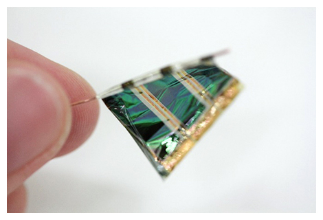
Flexible electronic skin equipped with an array of giant magneto resistance sensors and complex electronics circuit designed and developed for sensing distribution of magnetic field. Photo: Masaya Kondo

Researchers present the first fully integrated flexible electronics made of magnetic sensors and organic circuits which opens the path towards the development of electronic skin. Human skin is a fascinating and multifunctional organ with unique properties originating from its flexible and compliant nature. It allows for interfacing with external physical environment through numerous receptors interconnected with the nervous system. Scientists have been trying to transfer these features to artificial skin for a long time, aiming at robotic applications...

Read More

Well-designed Substrates make Large Single Crystal Bi-/Tri-Layer Graphene Possible

Figure 1. Preparation and characterization of Cu/Ni(111) foils.
Preparation and characterization of Cu/Ni(111) foils. (a) Schematic of the preparation of the Cu/Ni(111) foils shows that Ni films are electroplated on both sides of a Cu(111) foil, which is followed by heating in a chemical vapor deposition chamber at 1050 oC for 5-7 hours to obtain the Cu/Ni(111) foil. By controlling the concentration of nickel (Ni), IBS researchers could obtain bilayer and trilayer graphene with the desired stacking order and large area. (b) A photograph of a piece of Cu/Ni(111) alloy foil (3 cm × 5 cm in size). (c) X-ray pattern taken from different regions across the whole sample (3 cm × 5 cm). (d) Electron backscatter diffraction map indicating the uniform (111) orientation of the prepared Cu foils.

IBS researchers fabricate single crystal copper nickel alloy...

Read More

Billions of Quantum Entangled Electrons found in ‘Strange Metal’

Former Rice University graduate student Xinwei Li in 2016 with the terahertz spectrometer he later used to measure entanglement in the conduction electrons flowing through a “strange metal” compound of ytterbium, rhodium and silicon. (Photo by Jeff Fitlow/Rice University)

In a new study, U.S. and Austrian physicists have observed quantum entanglement among “billions of billions” of flowing electrons in a quantum critical material.

The research, which appears this week in Science, examined the electronic and magnetic behavior of a “strange metal” compound of ytterbium, rhodium and silicon as it both neared and passed through a critical transition at the boundary between two well-studied quantum phases.

The study at Rice University and Vienna University of Technology (TU Wien...

Read More