Category Technology/Electronics

New Material has Highest Electron Mobility among known Layered Magnetic materials

Atoms in layered material
High mobility in a van der Waals layered antiferromagnetic metal. Science Advances, 2020; 6 (6): eaay6407 DOI: 10.1126/sciadv.aay6407

A new material has properties that make it a promising candidate for new areas like magnetic twistronic devices and spintronics, as well as advances in data storage and device design.

All the elements are there to begin with, so to speak; it’s just a matter of figuring out what they are capable of – alone or together. For Leslie Schoop’s lab, one recent such investigation has uncovered a layered compound with a trio of properties not previously known to exist in one material.

With an international interdisciplinary team, Schoop, assistant professor of chemistry, and Postdoctoral Research Associate Shiming Lei, published a paper last week in Scien...

Read More
Cracks in Perovskite Films for Solar Cells easily Healed, study finds

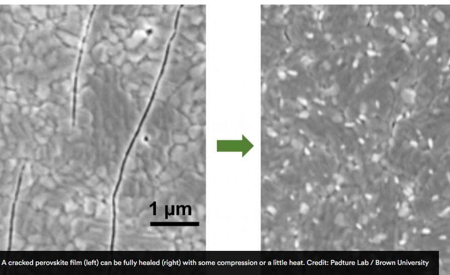
A cracked perovskite film (left) can be fully healed (right) with some compression or a little heat. Credit: Padture Lab / Brown University

A new study reveals good news for the possibility of using perovskite materials in next-generation solar cells. The study, published in the journal Acta Materialia, finds that though perovskite films tend to crack easily, those cracks are easily healed with some compression or a little bit of heat. That bodes well, the researchers say, for the use of inexpensive perovskites to replace or complement pricy silicon in solar cell technologies.

“The efficiency of perovskite solar cells has grown very quickly and now rivals silicon in laboratory cells,” said Nitin Padture, the Otis E...

Read More

New technology could help solve AI’s ‘Memory Bottleneck’

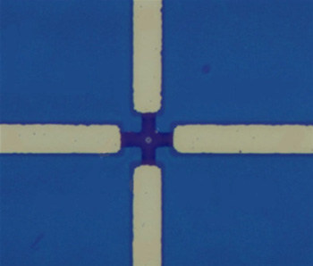
An optical image of the device structure with 4 micrometer pillar diameter. Credit: Northwestern University/University of Messina, Italy

Magnetic memory device is smallest demonstrated and uses record-low current. Memory-hungry, power-sapping big data might finally have met its match.

Electrical engineers at Northwestern University and the University of Messina in Italy have developed a new magnetic memory device that could potentially support the surge of data-centric computing, which requires ever-increasing power, storage and speed.

Based on antiferromagnetic (AFM) materials, the device is the smallest of its kind ever demonstrated and operates with record-low electrical current to write data.

“The rise of big data has enabled the emergence of artificial intelligence (AI)...

Read More

A Gold Butterfly can make its own Semiconductor Skin

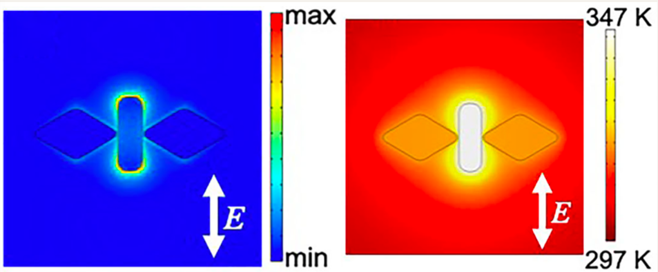
Calculated localized field (left) and temperature distribution (right) of the nano-butterfly structure. (Fujiwara H., et al, Nano Letters. December 23, 2019.)

A nanoscale gold butterfly provides a more precise route for growing/synthesizing nanosized semiconductors that can be used in nano-lasers and other applications.

Hokkaido University researchers have devised a unique approach for making nanosized semiconductors on a metal surface. The details of the method were reported in the journal Nano Letters and could further research into the fabrication of nanosized light and energy emitters.

The approach, developed by Hokkaido University’s Research Institute for Electronic Science and Hokkai-Gakuen University, involves generating localized heat on a gold nanoparticle within a ...

Read More