Category Technology/Electronics

New ‘Smart Needle’ to make Brain Surgery Safer

Smart needle which is able to detect blood vessels deep in the body. Credit: University of Adelaide

Smart needle which is able to detect blood vessels deep in the body. Credit: University of Adelaide

A new high-tech medical device to make brain surgery safer has been developed by researchers at the University of Adelaide. The tiny imaging probe, encased within a brain biopsy needle, lets surgeons ‘see’ at-risk blood vessels as they insert the needle, allowing them to avoid causing bleeds that can potentially be fatal. The project is a collaboration with the University of Western Australia and Sir Charles Gairdner Hospital. “We call it a smart needle...

Read More

New, Old Science Combine to Make Faster Medical Test

This is Assistant Professor Shawn Putnam of the University of Central Florida's College of Engineering & Computer Science. Credit: Courtesy University of Central Florida

This is Assistant Professor Shawn Putnam of the University of Central Florida’s College of Engineering & Computer Science. Credit: Courtesy University of Central Florida

Nanoparticles and Faraday rotation allow faster diagnoses. A UCF researcher has combined cutting-edge nanoscience with a magnetic phenomenon discovered more than 170 years ago to create a method for speedy medical tests. The discovery, if commercialized, could lead to faster test results for HIV, Lyme disease, syphilis, rotavirus and other infectious conditions. “I see no reason why a variation of this technique couldn’t be in every hospital throughout the world,” said Shawn Putnam, an assistant professor in the University of Central Florida’s College of Engineering & Computer Science.

At the core of the research are nanop...

Read More

Creating Atomic Scale nanoribbons

Researchers have made the first important step toward integrating atomically precise graphene nanoribbons (APGNRs) onto nonmetallic substrates. Credit: Adrian Radocea, Beckman Institute for Advanced Science and Technology

Researchers have made the first important step toward integrating atomically precise graphene nanoribbons (APGNRs) onto nonmetallic substrates. Credit: Adrian Radocea, Beckman Institute for Advanced Science and Technology

Researchers have demonstrated the first important step toward integrating atomically precise graphene nanoribbons (APGNRs) onto nonmetallic substrates. Silicon crystals are the semiconductors most commonly used to make transistors, which are critical electronic components used to carry out logic operations in computing. However, as faster and more powerful processors are created, silicon has reached a performance limit: the faster it conducts electricity, the hotter it gets, leading to overheating.

Graphene, made of a single-atom-thick sheet of carbon, stays much cooler a...

Read More

Explaining how 2D Materials Break at the Atomic level

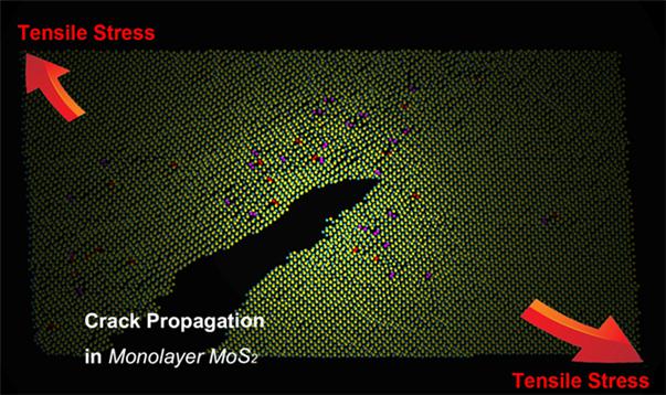
 Schematic representation of the crack propagation in 2D MoS2 at the atomic level. Dislocations shown with red and purple dots are visible at the crack tip zone. Internal tensile stresses are represented by red arrows.

Schematic representation of the crack propagation in 2D MoS2 at the atomic level. Dislocations shown with red and purple dots are visible at the crack tip zone. Internal tensile stresses are represented by red arrows.

Cracks sank the ‘unsinkable’ Titanic; decrease the performance of touchscreens and erode teeth. We are familiar with cracks in 3D objects, but how do thin 2D materials crack? 2D materials, like molybdenum disulfide (MoS2), have emerged as an important asset for future electronic and photoelectric devices. However, the mechanical properties of 2D materials are expected to differ greatly from 3D materials...

Read More