nanostructures tagged posts

Nanostructures enable On-Chip Lightwave-Electronic Frequency Mixer

Illustration of a computer chip, with waves of different colors and frequencies appearing above, below, and across it
The demonstration of a lightwave-electronic mixer at petahertz-scale frquencies is a first step toward making communication technology faster and progresses research toward developing new, miniaturized lightwave electronic circuitry capable of handling optical signals directly at the nanoscale.
Credits:Image: Sampson Wilcox/Research Laboratory of Electronics

Imagine how a phone call works: Your voice is converted into electronic signals, shifted up to higher frequencies, transmitted over long distances, and then shifted back down so it can be heard clearly on the other end. The process enabling this shifting of signal frequencies is called frequency mixing, and it is essential for communication technologies like radio and Wi-Fi...

Read More

The Metalens meets the Stars – Large, All-glass Metalens Images Sun, Moon and Nebulae

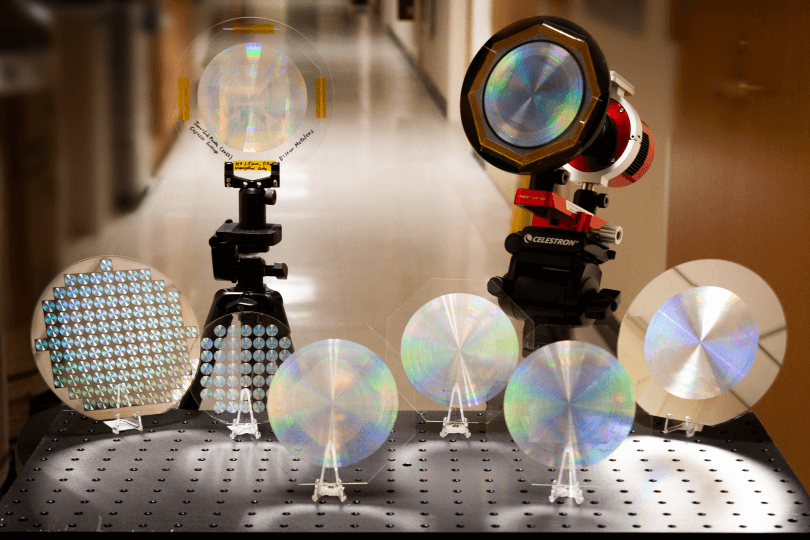
image of the metalens and camera
This 10-centimeter-diameter glass metalens can image the sun, the moon and distant nebulae with high resolution. (Credit: Capasso Lab/Harvard SEAS)
 

Metalenses have been used to image microscopic features of tissue and resolve details smaller than a wavelength of light. Now they are going bigger.

Researchers at the Harvard John A. Paulson School of Engineering and Applied Sciences (SEAS) have developed a 10-centimeter-diameter glass metalens that can image the sun, the moon and distant nebulae with high resolution.

It is the first all-glass, large-scale metalens in the visible wavelength that can be mass produced using conventional CMOS fabrication technology.

The research is published in ACS Nano.

“The ability to accurately control the size of tens of billions of nanopill...

Read More