

Metalenses have been used to image microscopic features of tissue and resolve details smaller than a wavelength of light. Now they are going bigger.
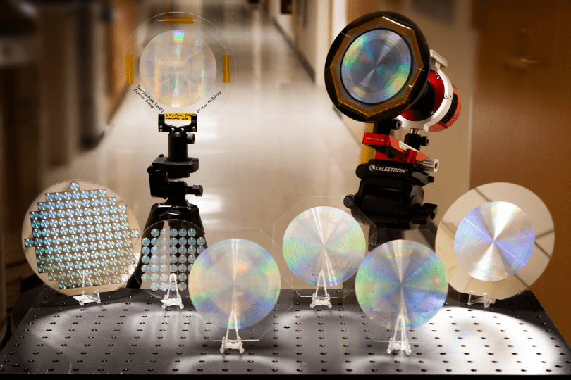
Researchers at the Harvard John A. Paulson School of Engineering and Applied Sciences (SEAS) have developed a 10-centimeter-diameter glass metalens that can image the sun, the moon and distant nebulae with high resolution.
It is the first all-glass, large-scale metalens in the visible wavelength that can be mass produced using conventional CMOS fabrication technology.
The research is published in ACS Nano.
“The ability to accurately control the size of tens of billions of nanopillars over an unprecedentedly large flat lens using state-of-the-art semiconductor foundry processes is a nanofabrication feat that opens exciting new opportunities for space science and technology,” said Federico Capasso, the Robert L. Wallace Professor of Applied Physics and Vinton Hayes Senior Research Fellow in Electrical Engineering at SEAS and senior author of the paper.
Most flat metalenses, which use millions of pillar-like nanostructures to focus light, are about the size of a piece of glitter.
In 2019, Capasso and his team developed a centimeter-scale metalens using a technique called deep-ultraviolet (DUV) projection lithography,which projects and forms a nanostructure pattern that can be directly etched into the glass wafer, eliminating the time-consuming writing and deposition processes that were required for previous metalenses.
DUV projection lithography is commonly used to pattern fine lines and shapes in silicon chips for smartphones and computers.
Joon-Suh Park, a former graduate student at SEAS and current postdoctoral fellow in Capasso’s team, demonstrated that the technique could not only be used to mass produce metalenses but also increase their size for applications in virtual and augmented reality.
But making the metalens even larger for applications in astronomy and free-space optical communications posed an engineering problem.
“There is a major limitation with the lithography tool because these tools are used to make computer chips, so chip size is restricted to no more than 20 to 30 millimeters,” said Park, co-first author of the paper.
“In order to make a 100-millimeter diameter lens, we needed to find a way around this limitation.”
Park and the team developed a technique to stitch together several patterns of nanopillars using the DUV projection lithography tool.
By dividing the lens into 25 sections but using only the 7 sections of a quadrant considering the rotational symmetry, the researchers showed that DUV projection lithography could pattern 18.7 billion designed nanostructures onto a 10-centimeter circular area in a matter of minutes. https://seas.harvard.edu/news/2024/01/metalens-meets-stars


Recent Comments