semiconductor tagged posts

Measuring a Tiny Quasiparticle is a major step forward for Semiconductor Technology

PL spectra of BN encapsulated monolayer WSe2 at 4.2 K. Credit: Nature Communications (2020). DOI: 10.1038/s41467-020-16934-x

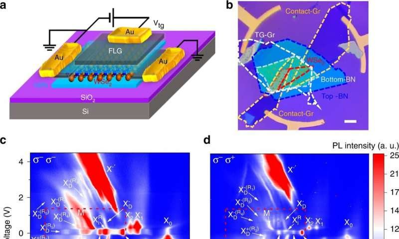
A team of researchers led by Sufei Shi, an assistant professor of chemical and biological engineering at Rensselaer Polytechnic Institute, has uncovered new information about the mass of individual components that make up a promising quasiparticle, known as an exciton, that could play a critical role in future applications for quantum computing, improved memory storage, and more efficient energy conversion.

Published today in Nature Communications, the team’s work brings researchers one step closer to advancing the development of semiconductor devices by deepening their understanding of an atomically thin class of materials known as transitional metal dichal...

Read More

Researchers Resolve a Major Mystery in 2D Material Electronics

Schematic drawing of a 2D-material-based lateral (left) and vertical (right) Schottky diode. For broad classes of 2D materials, the current-temperature relation can be universally described by a scaling exponent of 3/2 and 1, respectively, for lateral and vertical Schottky diodes. Credit: Singapore University of Technology and Design

Schematic drawing of a 2D-material-based lateral (left) and vertical (right) Schottky diode. For broad classes of 2D materials, the current-temperature relation can be universally described by a scaling exponent of 3/2 and 1, respectively, for lateral and vertical Schottky diodes.
Credit: Singapore University of Technology and Design

A one-size-fits-all master equation shall pave the way towards better design of 2D material electronics. Schottky diode is composed of a metal in contact with a semiconductor. Despite its simple construction, Schottky diode is a tremendously useful component and is omnipresent in modern electronics...

Read More

Atomically thin LED opens the possibility for ‘invisible’ displays

Gif of the device in action. Probes inject positive and negative charges in the light emitting device, which is transparent under the campanile outline, producing bright light. Credit: Javey lab

Gif of the device in action. Probes inject positive and negative charges in the light emitting device, which is transparent under the campanile outline, producing bright light. Credit: Javey lab

UC Berkeley engineers have built a bright-light emitting device that is millimeters wide and fully transparent when turned off. The light emitting material in this device is a monolayer semiconductor, just 3 atoms thick. The device opens the door to invisible displays on walls and windows – displays that would be bright when turned on but see-through when turned off – or in futuristic applications such as light-emitting tattoos, according to the researchers...

Read More

A Transistor of Graphene Nanoribbons: Breakthrough in Nanoelectronics

The microscopic ribbons lie criss-crossed on the gold substrate. Credit: EMPA

The microscopic ribbons lie criss-crossed on the gold substrate. Credit: EMPA

Transistors based on carbon nanostructures: what sounds like a futuristic dream could be reality in just a few years’ time. Scientists have now produced nanotransistors from graphene ribbons that are only a few atoms wide. Graphene ribbons have special electrical properties that make them promising candidates for the nanoelectronics of the future: While graphene is a conductive material, it can become a semiconductor in the form of nanoribbons. This means that it has a sufficiently large energy or band gap in which no electron states can exist: it can be turned on and off – and thus may become a key component of nanotransistors.

The smallest details in the atomic structure of these graphene bands, however, have m...

Read More