

Credit: Jianbo Liang, Osaka Metropolitan University
A research team at Osaka Metropolitan University has fabricated a gallium nitride (GaN) transistor using diamond, which of all natural materials has the highest thermal conductivity on earth, as a substrate, and they succeeded in increasing heat dissipation by more than 2X compared with conventional transistors. The transistor is expected to be useful not only in the fields of 5G communication base stations, weather radar, and satellite communications, but also in microwave heating and plasma processing.
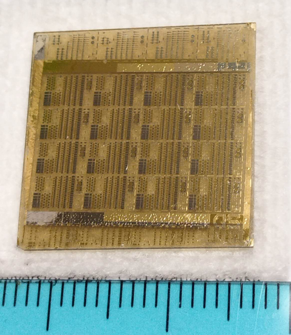
Researchers at Osaka Metropolitan University are proving that diamonds are so much more than just a ‘girl’s best friend.’ Their groundbreaking research focuses on gallium nitride (GaN) transistors, which are high-power, high-frequency semiconductor devices used in mobile data and satellite communication systems.
With the increasing miniaturization of semiconductor devices, problems arise such as increases in power density and heat generation that can affect the performance, reliability, and lifetime of these devices.
Therefore, effective thermal management is crucial. Diamond, which has the highest thermal conductivity of all natural materials, is an ideal substrate material but has not yet been put to practical use due to the difficulties of bonding diamond to GaN elements.
A research team led by Associate Professor Jianbo Liang and Professor Naoteru Shigekawa of the Graduate School of Engineering at Osaka Metropolitan University has successfully fabricated GaN High Electron Mobility Transistors using diamond as a substrate.
This novel technology has more than twice the heat dissipation performance of transistors of the same shape fabricated on a silicon carbide (SiC) substrate.
To maximize the high thermal conductivity of diamond, the researchers integrated a 3C-SiC layer, a cubic polytype of silicon carbide, between GaN and diamond.
This technique significantly reduces the thermal resistance of the interface and improves heat dissipation.
“This new technology has the potential to significantly reduce CO2 emissions and potentially revolutionize the development of power and radiofrequency electronics with improved thermal management capabilities,” said Professor Liang. https://www.omu.ac.jp/en/info/research-news/entry-42311.html


Recent Comments