
Category Physics

First Random Laser Made of Paper-based Ceramics

The team used conventional laboratory filter paper as a structural template due to its long fibers and the stable structure. Credit: Institute for Complex Systems /Rome

The team used conventional laboratory filter paper as a structural template due to its long fibers and the stable structure. Credit: Institute for Complex Systems /Rome

A team has built the first controllable random laser based on cellulose paper in Straubing. Hence, materials no longer need to be artificially outfitted with disordered structures, utilizing naturally occurring ones instead. Material synthesis that is inspired by biology is an area of research at TUM’s Chair of Biogenic Polymers at Straubing Center of Science. It utilizes models from nature and biogenic materials to develop new materials and technologies.

Two components are necessary for a laser: First of all, a medium which amplifies light. And secondly, a structure which retains the light in the medium...

Read More
The Thinnest Photodetector in the World

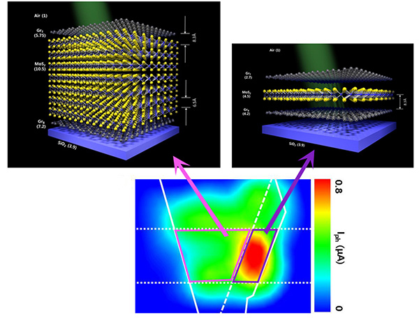
 (top) Devices with one-layer and seven-layer MoS2 were built on top of a silicon base and compared. Dielectric constants responsible for the difference in electrostatic potentials are shown in parenthesis. (bottom) The device with one-layer MoS2 (inside the violet box) showed better performance in converting light to electric current than the seven-layer device (inside the pink box).

(top) Devices with one-layer and seven-layer MoS2 were built on top of a silicon base and compared. Dielectric constants responsible for the difference in electrostatic potentials are shown in parenthesis. (bottom) The device with one-layer MoS2 (inside the violet box) showed better performance in converting light to electric current than the seven-layer device (inside the pink box).

The Center for Integrated Nanostructure Physics, within the Institute for Basic Science (IBS) has developed the world’s thinnest photodetector, that is a device that converts light into an electric current. With a thickness of just 1.3nm – 10X smaller than the current standard silicon diodes – this device could be used in the Internet of Things IoT, smart devices, wearable electronics and photoelectronics.

In ...

Read More

Computers made of Genetic Material? Researchers Conduct Electricity using DNA-based Nanowires

Scientists at Helmholtz-Zentrum Dresden-Rossendorf conducted electricity through DNA-based nanowires by placing gold-plated nanoparticles on them. In this way it could become possible to develop circuits based on genetic material. Credit: Image courtesy of Helmholtz-Zentrum Dresden-Rossendorf

Scientists at Helmholtz-Zentrum Dresden-Rossendorf conducted electricity through DNA-based nanowires by placing gold-plated nanoparticles on them. In this way it could become possible to develop circuits based on genetic material. Credit: Image courtesy of Helmholtz-Zentrum Dresden-Rossendorf

Tinier than the AIDS virus—that is currently the circumference of the smallest transistors. The industry has shrunk the central elements of their computer chips to 14nm in the last 60 years. Conventional methods, however, are hitting physical boundaries. Researchers around the world are looking for alternatives. One method could be the self-organization of complex components from molecules and atoms...

Read More

Close to Absolute Zero, Electrons exhibit their Quantum Nature

Keeping a close eye on everything: Christian Ast checks the connections of the scanning tunneling microscope (top). Researchers in the Nanoscale Science Department conduct their experiments in this instrument at lowest temperatures of a fifteen thousandth of a degree above absolute zero. The principle is always the same (bottom): A tunneling current (illustrated by the transparent bar) flows between an ultrafine tip and the sample, providing information about the properties of the sample. At these low temperatures the tunneling current reveals all of its quantum properties.

Keeping a close eye on everything: Christian Ast checks the connections of the scanning tunneling microscope (top). Researchers in the Nanoscale Science Department conduct their experiments in this instrument at lowest temperatures of a fifteen thousandth of a degree above absolute zero. The principle is always the same (bottom): A tunneling current (illustrated by the transparent bar) flows between an ultrafine tip and the sample, providing information about the properties of the sample. At these low temperatures the tunneling current reveals all of its quantum properties. Credit: Tom Pingel (top), MPI for Solid State Research (bottom)

What would happen if an electric current no longer flowed, but trickled instead? This was the question investigated by researchers working with Christian ...

Read More