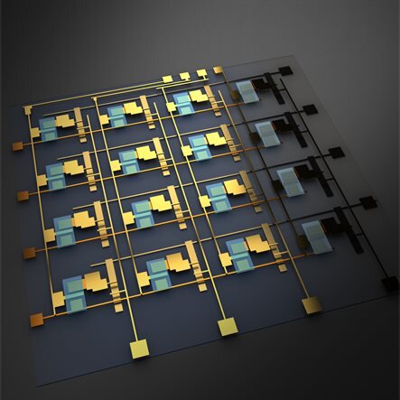
Category Technology/Electronics

Scalable Method to Manufacture Thin Film Transistors achieves Ultraclean Interface

Scalable method to manufacture thin film transistors achieves ultra-clean interface for high performance, low-voltage device ope
Microchip containing thin film transistors having record sub-threshold slope, made using the in situ atomic layer deposition process. Credit: Silvia Cardarelli, Michigan ECE

Prof. Becky Peterson at the University of Michigan leads a team that has developed a scalable, manufacturable method for developing thin film transistors (TFTs) that operate at the lowest possible voltage. This is particularly important for TFT integration with today’s silicon complementary metal-oxide semiconductors (CMOS), which are used in the vast majority of integrated circuits.

“We’re essentially developing a less complicated device that operates at lower voltage,” said ECE Ph.D. student Tonglin (Tanya) Newsom, who is first author on the paper...

Read More

Spin Transport Measured through Molecular Films now long enough to develop Spintronic Devices

Schematic illustration of the spin transport demonstration of αNPD molecular thin film

Materials breakthrough in microfabrication could lead to a new generation of smaller, faster, energy-efficient electronics. A research group has succeeded in measuring spin transport in a thin film of specific molecules — a material well-known in organic light emitting diodes — at room temperature. They found that this thin molecular film has a spin diffusion length of approximately 62 nm, a length that could have practical applications in developing spintronics technology. In addition, while electricity has been used to control spin transport in the past, the thin molecular film used in this study is photoconductive, allowing spin transport control using visible light.

Information processing dev...

Read More

New Antennas and Microchips help Electronics blur the line between Science and Sci-fi

Kaushik Sengupta in his lab at Princeton
Researchers in Kaushik Sengupta’s lab work to expand the capabilities of modern electronics. Photos by Sameer A. Khan/Fotobuddy

Sophisticated antenna arrays paired with high-frequency wireless chips act like superpowers for modern electronics, boosting everything from sensing to security to data processing. In his lab at Princeton, Kaushik Sengupta is working to expand those powers even further.

In recent years, Sengupta’s lab has designed antenna arrays that help engineers make strides toward peering through matter, boosting communications in canyons of skyscrapers, putting a medical lab on a smart phone, and encrypting critical data with electromagnetic waves instead of software.

In a new article in Advanced Science, Sengupta’s research team presented a new type of antenna arra...

Read More

Approaching the Terahertz Regime

(Left) A chaotic greyscale rectangle. (Right) Isometric view of colored layers sandwiched together.
Antiferromagnetic tunneling junction. High-resolution transmission electron microscopy image of the antiferromagnetic junction showing layers of different materials (left). Diagram showing the materials’ magnetic properties (right). ©2023 Nakatsuji et al. CC-BY

Room temperature quantum magnets switch states trillions of times per second. A class of nonvolatile memory devices, called MRAM, based on quantum magnetic materials, can offer a thousandfold performance beyond current state-of-the-art memory devices. The materials known as antiferromagnets were previously demonstrated to store stable memory states, but were difficult to read from. This new study paves an efficient way for reading the memory states, with the potential to do so incredibly quickly too.

You can probably blink...

Read More