Category Technology/Electronics

Performing Matrix Multiplications at the Speed of Light for Enhanced Cybersecurity

Matrix multiplications at the speed of light
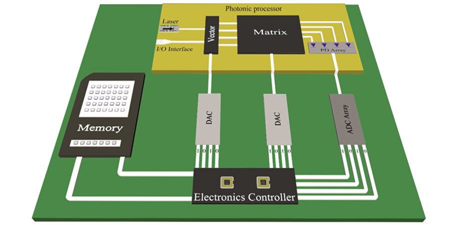
Electro-optic blocks cointegrated for the development of a neuromorphic photonic processor. Credit: Giamougiannis et al., doi 10.1117/1.AP.5.1.016004

“All things are numbers,” avowed Pythagoras. Today, 25 centuries later, algebra and mathematics are everywhere in our lives, whether we see them or not. The Cambrian-like explosion of artificial intelligence (AI) brought numbers even closer to us all, since technological evolution allows for parallel processing of a vast amounts of operations.

Progressively, operations between scalars (numbers) were parallelized into operations between vectors, and subsequently, matrices. Multiplication between matrices now trends as the most time- and energy-demanding operation of contemporary AI computational systems...

Read More
Superconductivity Switches On and Off in ‘Magic-Angle’ Gaphene

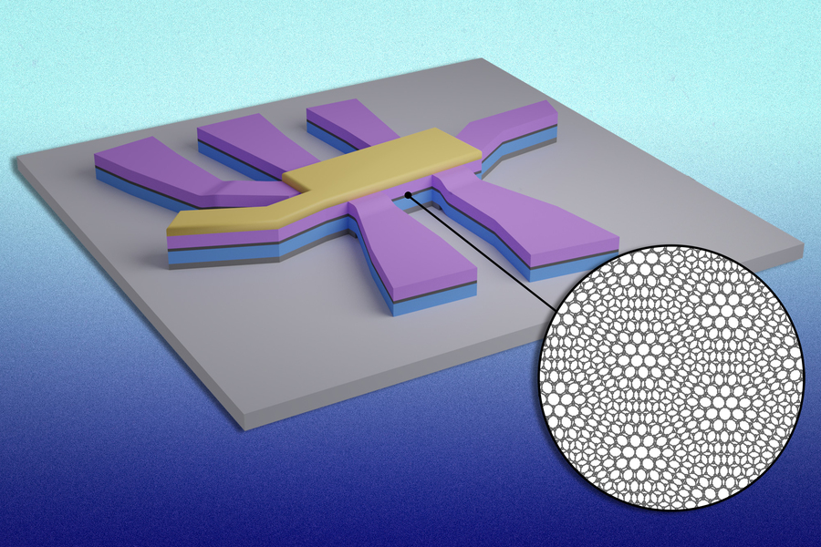
A unique device is made of sandwiched layers, with yellow and purple on top and blue on bottom. The middle layer is dark grey representing 2 layers of graphene, and the inset shows the graphene layers creating a moiré pattern. The device has a central rectangular shape with 7 more rectangular shapes emanating from it.
Caption:MIT physicists have found a new way to switch superconductivity on and off in magic-angle graphene. This figure shows a device with two graphene layers in the middle (in dark gray and in inset). The graphene layers are sandwiched in between boron nitride layers (in blue and purple). The angle and alignment of each layer enables the researchers to turn superconductivity on and off in graphene with a short electric pulse.
Credits:Credit: Courtesy of the researchers. Edited by MIT News.

A quick electric pulse completely flips the material’s electronic properties, opening a route to ultrafast, brain-inspired, superconducting electronics...

Read More

Scalable Method to Manufacture Thin Film Transistors achieves Ultraclean Interface

Scalable method to manufacture thin film transistors achieves ultra-clean interface for high performance, low-voltage device ope
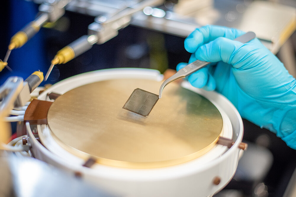
Microchip containing thin film transistors having record sub-threshold slope, made using the in situ atomic layer deposition process. Credit: Silvia Cardarelli, Michigan ECE

Prof. Becky Peterson at the University of Michigan leads a team that has developed a scalable, manufacturable method for developing thin film transistors (TFTs) that operate at the lowest possible voltage. This is particularly important for TFT integration with today’s silicon complementary metal-oxide semiconductors (CMOS), which are used in the vast majority of integrated circuits.

“We’re essentially developing a less complicated device that operates at lower voltage,” said ECE Ph.D. student Tonglin (Tanya) Newsom, who is first author on the paper...

Read More

Spin Transport Measured through Molecular Films now long enough to develop Spintronic Devices

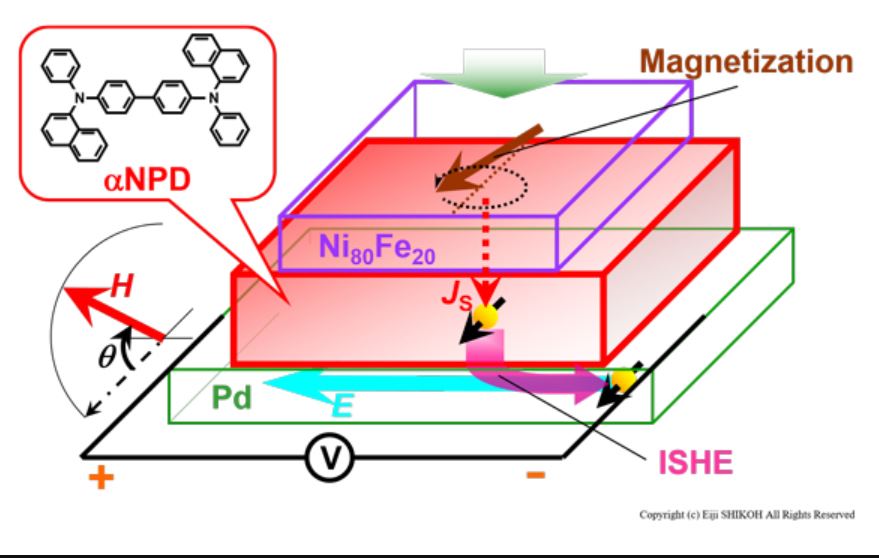
Schematic illustration of the spin transport demonstration of αNPD molecular thin film

Materials breakthrough in microfabrication could lead to a new generation of smaller, faster, energy-efficient electronics. A research group has succeeded in measuring spin transport in a thin film of specific molecules — a material well-known in organic light emitting diodes — at room temperature. They found that this thin molecular film has a spin diffusion length of approximately 62 nm, a length that could have practical applications in developing spintronics technology. In addition, while electricity has been used to control spin transport in the past, the thin molecular film used in this study is photoconductive, allowing spin transport control using visible light.

Information processing dev...

Read More