
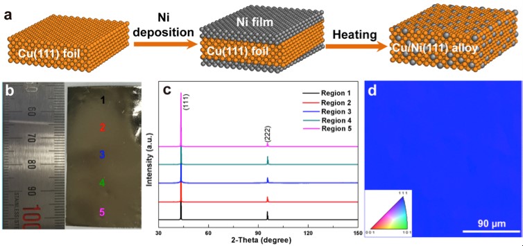
IBS researchers fabricate single crystal copper nickel alloy...
Read More

January 22, 2020,
 Physics, Technology/Electronics, Chemistry/Nanotechnology
IBS researchers fabricate single crystal copper nickel alloy...
Read More
January 17, 2020,
Physics, Technology/Electronics
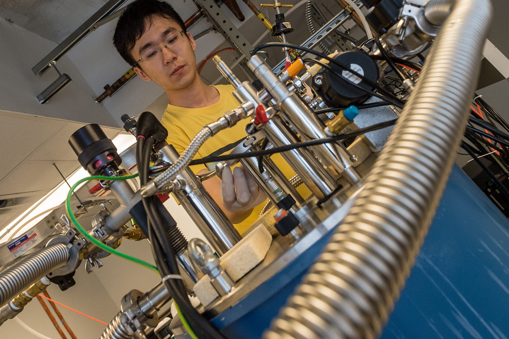
In a new study, U.S. and Austrian physicists have observed quantum entanglement among “billions of billions” of flowing electrons in a quantum critical material.
The research, which appears this week in Science, examined the electronic and magnetic behavior of a “strange metal” compound of ytterbium, rhodium and silicon as it both neared and passed through a critical transition at the boundary between two well-studied quantum phases.
The study at Rice University and Vienna University of Technology (TU Wien...
Read More
January 17, 2020,
Physics, Technology/Electronics, Environment/Geology

Printed circuit boards are vital components of modern electronics. However, once they have served their purpose, they are often burned or buried in landfills, polluting the air, soil and water. Most concerning are the brominated flame retardants added to printed circuit boards to keep them from catching fire. Now, researchers reporting in ACS Sustainable Chemistry & Engineering have developed a ball-milling method to break down these potentially harmful compounds, enabling safer disposal.
Composed of 30% metallic and 70% nonmetallic particles, printed circuit boards support and connect all of the electrical components of a device...
Read More
January 16, 2020,
Physics, Technology/Electronics

Los Alamos scientists have incorporated meticulously engineered colloidal quantum dots into a new type of light emitting diodes (LEDs) containing an integrated optical resonator, which allows them to function as lasers. These novel, dual-function devices clear the path towards versatile, manufacturing-friendly laser diodes. The technology can potentially revolutionize numerous fields from photonics and optoelectronics to chemical sensing and medical diagnostics.
“This latest breakthrough along with other recent advances in quantum dot chemistry and device engineering that we have achieved suggest that laser diodes assembled from solution may soon become a reality,” said Victor Klimov, head of the quantum dot group at Los Alamos Nationa...
Read More
Recent Comments