
Category Technology/Electronics

2D Electronics’ Metal or Semiconductor? Both

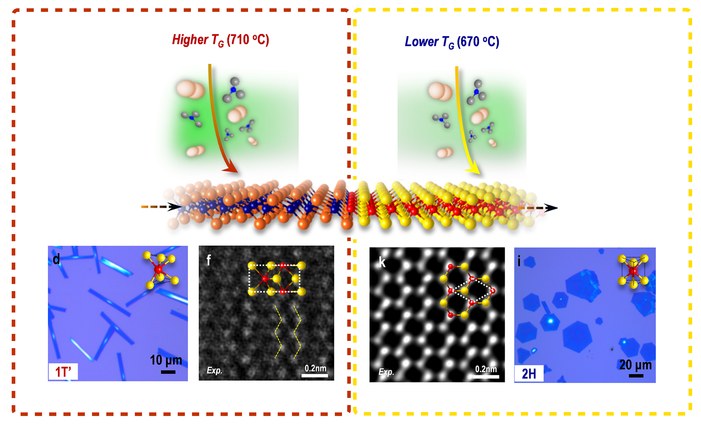
Molybdenum telluride (MoTe2) polymorphism. Metallic (right) and semiconducting (left) MoTe2 crystals are obtained side by side on the same plane. Rectangular crystals represent metal MoTe2, while hexagonal crystals are the characteristic feature of semiconducting MoTe2.

Molybdenum telluride (MoTe2) polymorphism. Metallic (right) and semiconducting (left) MoTe2 crystals are obtained side by side on the same plane. Rectangular crystals represent metal MoTe2, while hexagonal crystals are the characteristic feature of semiconducting MoTe2.

Researchers produced the first 2D field-effect transistor (FET) made of a single material. Modern life will be almost unthinkable without transistors. They are the ubiquitous building blocks of all electronic devices: each computer chip contains billions of them. However, as the chips become smaller and smaller, the current 3D field-electronic transistors (FETs) are reaching their efficiency limit...

Read More

Chemists Make Playdough/ Lego-like Hybrid to create Tiny Building Blocks

Computer renderings illustrating the design of micro-structured patchy particles. These tiny objects (1/4th of the size a red blood cell) are first created inside a computer using simulations and then fabricated in the laboratory. Image courtesy of Theodore Hueckel.

Computer renderings illustrating the design of micro-structured patchy particles. These tiny objects (1/4th of the size a red blood cell) are first created inside a computer using simulations and then fabricated in the laboratory. Image courtesy of Theodore Hueckel.

Playdough and Legos are among the most popular childhood building blocks. But what could you use if you wanted to create something really small – a structure less than the width of a human hair? It turns out, a team of chemists has found, this can be achieved by creating particles that have both playdough and Lego traits. These “patchy particles,” described in the latest issue of the journal Nature, are 1/200th the width of a human hair and can form endless architectures from a handful of basic pieces...

Read More

Wireles High-Speed Data and Power Transfer Integrated

Ultra-high Data-rate Communication and Efficient Wireless Power Transfer at 13.56 MHz. IEEE Antennas and Wireless Propagation Letters, 2017; 1 DOI: 10.1109/LAWP.2017.2736883

Ultra-high Data-rate Communication and Efficient Wireless Power Transfer at 13.56 MHz. IEEE Antennas and Wireless Propagation Letters, 2017; 1 DOI: 10.1109/LAWP.2017.2736883

North Carolina State University researchers have developed a system that can simultaneously deliver watts of power and transmit data at rates high enough to stream video over the same wireless connection. By integrating power and high-speed data, a true single “wireless” connection can be achieved. A/Prof David Ricketts said: “One of the most popular applications is in wireless cell phone charging pads. As many know, these unfortunately often require almost physical contact with the pad, limiting the usefulness of a truly ‘wireless’ power source...

Read More

World 1st: ‘Storing Lightning inside Thunder’

Basic principle and setup of the photonic–phononic memory. a Storing process: an optical data pulse is depleted by a strong counter-propagating write pulse, storing the data pulse as an acoustic phonon. b Retrieval process: in the retrieval process a read pulse depletes the acoustic wave, converting the data pulse back into the optical domain. c A basic schematic of the experimental setup. The inset shows a chalcogenide chip next to a 50-cent coin. The chip contains more than 100 spiral waveguides with different lengths (8.6, 11.7 and 23.7 cm). Note: this is only a schematic and the actual setup is more advanced and can be found in Supplementary Fig. 1 (CW continuous wave, SSB single-sideband modulator, IM intensity modulator, PG pulse generator, BP bandpass filter, PD photo-detector, LO local oscillator, Ω Brillouin frequency shift)

Basic principle and setup of the photonic–phononic memory. a Storing process: an optical data pulse is depleted by a strong counter-propagating write pulse, storing the data pulse as an acoustic phonon. b Retrieval process: in the retrieval process a read pulse depletes the acoustic wave, converting the data pulse back into the optical domain. c A basic schematic of the experimental setup. The inset shows a chalcogenide chip next to a 50-cent coin. The chip contains more than 100 spiral waveguides with different lengths (8.6, 11.7 and 23.7 cm). Note: this is only a schematic and the actual setup is more advanced and can be found in Supplementary Fig...

Read More