


Iowa State engineers are developing real-world, low-cost applications for graphene. Credit: Photos by Christopher Gannon/Iowa State University.
Engineers have used laser-treatment process that allows them to use printed graphene for electric circuits and electrodes – even on paper and other fragile surfaces. The technology could lead to many real-world, low-cost applications for printed graphene electronics, including sensors, fuel cells and medical devices. Previous technology meant that graphene had to be treated to improve electrical conductivity and device performance. That usually meant high temperatures or chemicals – both could degrade flexible or disposable printing surfaces such as plastic films or even paper.
Das PhD and assistant/Prof Claussen came up with the idea of using lasers to treat the graphene. They found treating inkjet-printed, multi-layer graphene electric circuits and electrodes with a pulsed-laser process improves electrical conductivity without damaging paper, polymers or other fragile printing surfaces. “This creates a way to commercialize and scale-up the manufacturing of graphene,” Claussen said.
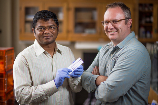
Suprem Das holds graphene electronics printed on a sheet of paper. Das and Jonathan Claussen, right, are using lasers to treat the printed graphene electronics. The process improves conductivity and enables flexible, wearable and low-cost electronics. Photos by Christopher Gannon.
The Iowa State Research Foundation Inc. has filed for a patent on the technology. “The breakthrough of this project is transforming the inkjet-printed graphene into a conductive material capable of being used in new applications,” Claussen said. Those applications could include sensors with biological applications, energy storage systems, electrical conducting components and even paper-based electronics.
To make all that possible, the engineers developed computer-controlled laser technology that selectively irradiates inkjet-printed graphene oxide. The treatment removes ink binders and reduces graphene oxide to graphene – physically stitching together millions of tiny graphene flakes. The process makes electrical conductivity more than a 1000X better. “The laser works with a rapid pulse of high-energy photons that do not destroy the graphene or the substrate,” Das said. “They heat locally. They bombard locally. They process locally.”
That localized, laser processing also changes the shape and structure of the printed graphene from a flat surface to one with raised, 3D nanostructures.The rough and ridged structure increases the electrochemical reactivity of the graphene, making it useful for chemical and biological sensors.
All of that, according to Claussen’s team of nanoengineers, could move graphene to commercial applications. “This work paves the way for not only paper-based electronics with graphene circuits,” the researchers wrote in their paper, “it enables the creation of low-cost and disposable graphene-based electrochemical electrodes for myriad applications including sensors, biosensors, fuel cells and (medical) devices.” http://www.news.iastate.edu/news/2016/09/01/paperelectronics


Recent Comments