CMOS tagged posts

Wirelessly Powered Relay will help bring 5G Technology to Smart Factories

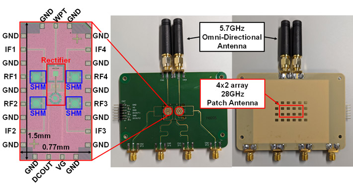
Figure 2 Prototype of the proposed relay transceiver The prototype of the proposed relay transceiver was fabricated with Si CMOS 65nm chips and 4×2 patch phased-array antenna board.
Prototype of the proposed relay transceiver
The prototype of the proposed relay transceiver was fabricated with Si CMOS 65nm chips and 4×2 patch phased-array antenna board.

The proposed innovative design leads to unprecedented power conversion efficiency and improved versatility. A recently developed wirelessly powered 5G relay could accelerate the development of smart factories, report scientists from Tokyo Tech. By adopting a lower operating frequency for wireless power transfer, the proposed relay design solves many of the current limitations, including range and efficiency. In turn, this allows for a more versatile and widespread arrangement of sensors and transceivers in industrial settings.

One of the hallmarks of the Information Age is the transformation of industries towards...

Read More

World’s first N-Channel Diamond Field-Effect Transistor for CMOS Integrated Circuits

World's first N-channel diamond field-effect transistor for CMOS integrated circuits

A National Institute for Materials Science (NIMS) research team has developed the world’s first n-channel diamond MOSFET (metal-oxide-semiconductor field-effect transistor). The developed n-channel diamond MOSFET provides a key step toward CMOS (complementary metal-oxide-semiconductor: one of the most popular technologies in the computer chip) integrated circuits for harsh environment applications, as well as the development of diamond power electronics. The research is published in Advanced Science.

Semiconductor diamond has outstanding physical properties such as ultra wide-bandgap energy of 5...

Read More

The Metalens meets the Stars – Large, All-glass Metalens Images Sun, Moon and Nebulae

image of the metalens and camera
This 10-centimeter-diameter glass metalens can image the sun, the moon and distant nebulae with high resolution. (Credit: Capasso Lab/Harvard SEAS)
 

Metalenses have been used to image microscopic features of tissue and resolve details smaller than a wavelength of light. Now they are going bigger.

Researchers at the Harvard John A. Paulson School of Engineering and Applied Sciences (SEAS) have developed a 10-centimeter-diameter glass metalens that can image the sun, the moon and distant nebulae with high resolution.

It is the first all-glass, large-scale metalens in the visible wavelength that can be mass produced using conventional CMOS fabrication technology.

The research is published in ACS Nano.

“The ability to accurately control the size of tens of billions of nanopill...

Read More

Conjoined ‘Racetracks’ make new Optical Device possible

Credit: Brian Long

Kerry Vahala and collaborators from UC Santa Barbara have found a unique solution to an optics problem. When we last checked in with Caltech’s Kerry Vahala three years ago, his lab had recently reported the development of a new optical device called a turnkey frequency microcomb that has applications in digital communications, precision time keeping, spectroscopy, and even astronomy.

This device, fabricated on a silicon wafer, takes input laser light of one frequency and converts it into an evenly spaced set of many distinct frequencies that form a train of pulses whose length can be as short as 100 femtoseconds (quadrillionths of a second). (The comb in the name comes from the frequencies being spaced like the teeth of a hair comb.)

Now Vahala (BS ’80, MS ’81,...

Read More