A National Institute for Materials Science (NIMS) research team has developed the world’s first n-channel diamond MOSFET (metal-oxide-semiconductor field-effect transistor). The developed n-channel diamond MOSFET provides a key step toward CMOS (complementary metal-oxide-semiconductor: one of the most popular technologies in the computer chip) integrated circuits for harsh environment applications, as well as the development of diamond power electronics. The research is published in Advanced Science.
Semiconductor diamond has outstanding physical properties such as ultra wide-bandgap energy of 5.5 eV, high carriers mobilities, and high thermal conductivity, which is promising for the applications under extreme environmental conditions with high performance and high reliability, such as the environments with high temperatures and high levels of radiation (e.g., in proximity to nuclear reactor cores).
By using diamond electronics, not only can the thermal management demand for conventional semiconductors be alleviated but these devices are also more energy efficient and can endure much higher breakdown voltages and harsh environments.
With the development of diamond growth technologies, power electronics, spintronics, and microelectromechanical system (MEMS) sensors operatable under high-temperature and strong-radiation conditions, the demand for peripheral circuitry based on diamond CMOS devices has increased for monolithic integration.
For the fabrication of CMOS integrated circuits, both p- and n-type channel MOSFETs are required for conventional silicon electronics. However, n-channel diamond MOSFETs had yet to be developed.
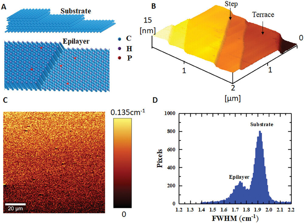
This NIMS research team developed a technique to grow high-quality monocrystalline n-type diamond semiconductors with smooth and flat terraces at the atomic level by doping diamond with a low concentration of phosphorus.
Using this technique, the team succeeded in fabricating an n-channel diamond MOSFET for the first time in the world. This MOSFET is composed mainly of an n-channel diamond semiconductor layer atop another diamond layer doped with a high concentration of phosphorus.
The use of the latter diamond layer significantly reduced source and drain contact resistance. The team confirmed that the fabricated diamond MOSFET actually functioned as an n-channel transistor.
In addition, the team verified the excellent high-temperature performance of the MOSFET as indicated by its field-effect mobility—an important transistor performance indicator—of approximately 150 cm2/V・sec at 300°C.
These achievements are expected to facilitate the development of CMOS integrated circuits for the manufacture of energy-efficient power electronics, spintronic devices and (MEMS) sensors under harsh environments. https://techxplore.com/news/2024-03-world-channel-diamond-field-effect.html


Recent Comments