transistors tagged posts

3D silicon circuits bring denser computer chips closer to reality

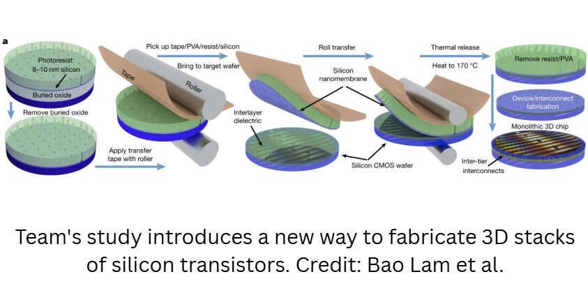
By stacking transistors on top of one another, rather than laying them side by side on a flat chip, many electronic engineers are hopeful that vast amounts of computing power could be packed into tiny spaces, all while cutting energy use. So far, however, the ability to build these monolithic 3D integrated circuits has proven stubbornly difficult, largely because the fabrication processes required can damage the layers already in place.

Through new research published in Nature, Qing Cao and colleagues at the University of Illinois Urbana-Champaign have developed a new approach that sidesteps these problems, bringing high-performance 3D chips a step closer to reality.

Overheated stacks of transistors
Modern computer chips are built on thin wafers of silicon, with transistors (the ...

Read More

New Molecular Device has unprecedented Reconfigurability reminiscent of Brain-Plasticity

Decision trees within a molecular memristor | Nature
Fig. 1: Circuit element structure and I(V) characteristics

Device can be reconfigured multiple times simply by changing applied voltage. In a discovery published in the journal Nature, an international team of researchers has described a novel molecular device with exceptional computing prowess.

Reminiscent of the plasticity of connections in the human brain, the device can be reconfigured on the fly for different computational tasks by simply changing applied voltages. Furthermore, like nerve cells can store memories, the same device can also retain information for future retrieval and processing.

“The brain has the remarkable ability to change its wiring around by making and breaking connections between nerve cells...

Read More

Fast Material Manipulation Through a Laser

A femtosecond burst of light drives an exotic electronic transition in a semi-metallic crystal, on an unprecedently fast timescale.
© Beaulieu

Researchers from the Physical Chemistry Department of the Fritz Haber Institute and the Max Planck Institute for the Structure and Dynamics of Matter in Hamburg have found out that ultrafast switches in material properties can be prompted by laser pulses – and why. This knowledge may enable new transistor concepts.

Making the speed of electronic technology as fast as possible is a central aim of contemporary materials research. The key components of fast computing technologies are transistors: switching devices that turn electrical currents on and off very quickly as basic steps of logic operations...

Read More

Putty-like Composites of Gallium metal with potential for Real-World Application

Figure 1.
(a) Liquid gallium being poured into a container. (b) Gallium putty being molded into a ball. (c) Various figures made from gallium putty. (d) Gallium putty being cut by a blade. (e) The mechanism of formation of gallium putty involves filler particles being encapsulated by a gallium oxide layer and incorporated into the gallium.

Researchers created a novel functional composite of gallium with putty or paste-like physical properties. The composite possesses excellent electromagnetic shielding as well as thermal conductivity. Gallium is a highly useful element that has accompanied the advancement of human civilization throughout the 20th century. Gallium is designated as a technologically critical element, as it is essential for the fabrication of semiconductors and transistors...

Read More