

By stacking transistors on top of one another, rather than laying them side by side on a flat chip, many electronic engineers are hopeful that vast amounts of computing power could be packed into tiny spaces, all while cutting energy use. So far, however, the ability to build these monolithic 3D integrated circuits has proven stubbornly difficult, largely because the fabrication processes required can damage the layers already in place.
Through new research published in Nature, Qing Cao and colleagues at the University of Illinois Urbana-Champaign have developed a new approach that sidesteps these problems, bringing high-performance 3D chips a step closer to reality.
Overheated stacks of transistors
Modern computer chips are built on thin wafers of silicon, with transistors (the tiny switches that process information) arranged in a single flat layer. If multiple layers of transistors could instead be stacked on top of each other on the same chip, it would dramatically increase their density without enlarging the chip’s footprint. However, this 3D design would cause the chip to overheat, which could destroy the circuitry already laid down beneath it.
To address this challenge, several studies have tried to replace the silicon used in conventional transistors with alternative materials, which can be processed at lower temperatures. However, these designs have consistently underperformed compared with their silicon counterparts, largely canceling out the benefits of going 3D.
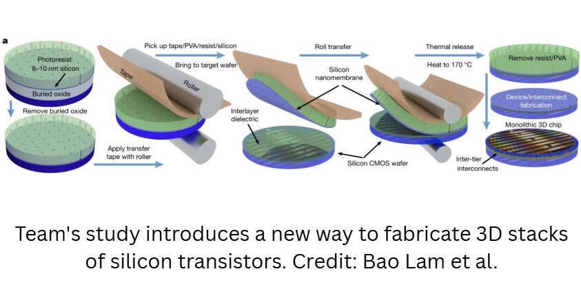
Innovative new design
In their study, Cao’s team found a way to keep silicon while working within the tight temperature constraints that 3D stacking demands. Their key innovation is the use of extremely thin, flexible sheets of silicon just 10 nanometers thick, which they transferred onto the chip using a roller.
The sheets are peeled from a specialized silicon substrate using adhesive tape and then rolled into place at temperatures below 200 °C—well within safe limits for the layers below. Because the sheets are flexible, they conform comfortably to the surface beneath, producing a uniform bond even if that surface isn’t perfectly flat.
Finally, the team patterned the transistors onto each silicon sheet using a design that avoids the high-temperature steps required by conventional transistors.
Sticking with silicon
The resulting devices match up well with standard silicon transistors in terms of how efficiently they carry current, and successive layers can be aligned to within less than ten nanometers of each other: a level of precision essential for dense, reliable circuitry.
With this approach, Cao’s team were able to build working three-layer memory cells, reducing the circuit’s footprint by up to three times compared with an equivalent flat design.
The results suggest that high-performance silicon wouldn’t need to be sacrificed in the move to 3D chips. For now, scaling the process up to the larger wafer sizes used in industrial chip production remains a significant engineering challenge—but all the same, the work marks a promising step towards denser, more capable integrated circuits built from a material the industry already knows how to use. https://techxplore.com/news/2026-05-3d-silicon-circuits-denser-chips.html


Recent Comments